Silicon carbide MOSFET high-temperature gate bias test method

A high-temperature gate bias and testing method technology, which is applied in the direction of single semiconductor device testing, etc., can solve problems such as SiC MOSFET thermal runaway, threshold voltage drift, etc., and achieve the effect of in-situ testing

Inactive Publication Date: 2019-05-21
NO 55 INST CHINA ELECTRONIC SCI & TECHNOLOGYGROUP CO LTD
View PDF5 Cites 10 Cited by
  • Summary
  • Abstract
  • Description
  • Claims
  • Application Information

AI Technical Summary

Problems solved by technology

[0005] Since SiC MOSFETs are prone to thermal runaway, and the threshold voltage will drift significantly during the device test process, the high temperature gate bias test and its electrical test results are heavily dependent on the test conditions, such as the length of the test time interval after the high temperature gate bias test, the gate Factors such as electrode voltage scanning mode and test temperature will seriously affect the test results. According to the current high-temperature gate bias test conditions and post-test electrical measurement conditions specified in JEDEC JESD-22A108C, wrong conclusions may be obtained. The high-temperature gate bias test method for silicon MOSFETs It is not completely suitable for silicon carbide MOSFET devices, so it is necessary to study the high temperature gate bias test method for silicon carbide MOSFETs to form a test method suitable for SiC MOSFET devices

Method used


Image

  • Silicon carbide MOSFET high-temperature gate bias test method
  • Silicon carbide MOSFET high-temperature gate bias test method
  • Silicon carbide MOSFET high-temperature gate bias test method

Examples


Embodiment

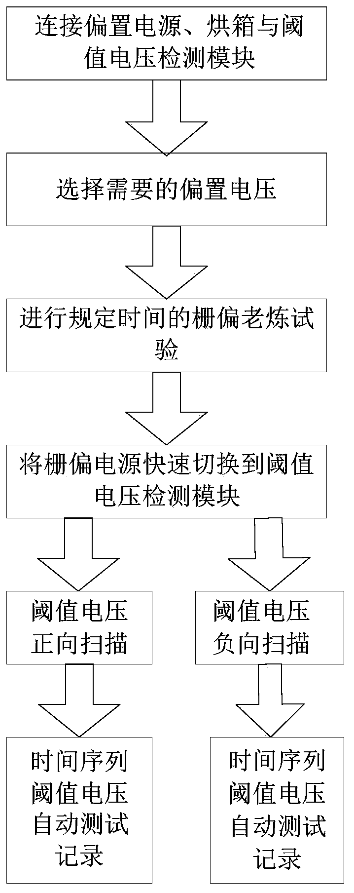
[0031] Such as figure 1 As shown, a silicon carbide MOSFET high temperature gate bias test method includes the following steps:

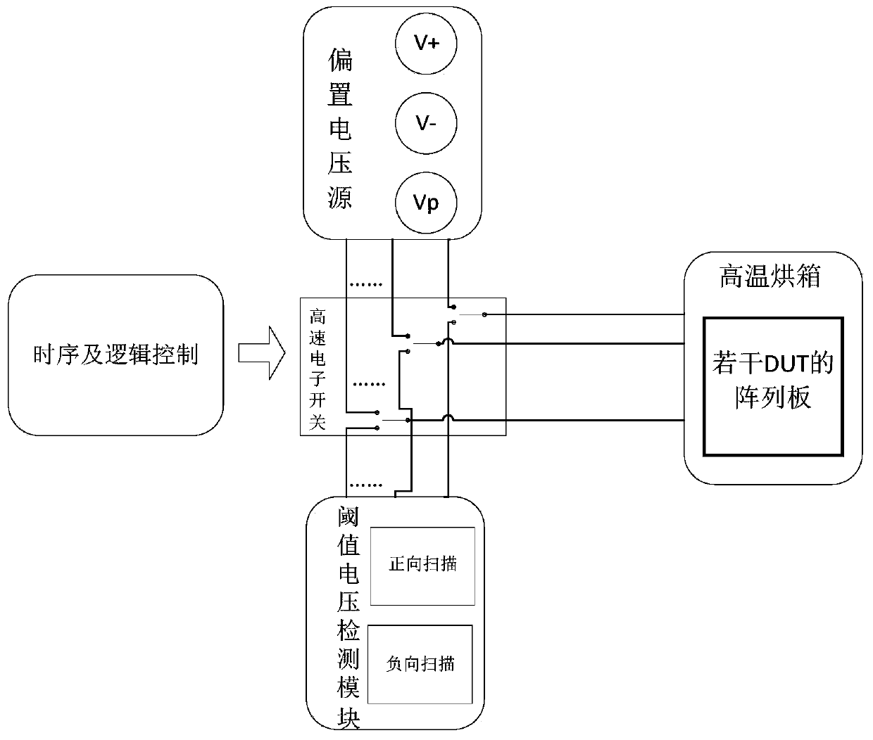
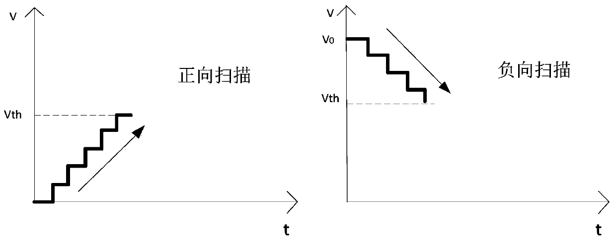
[0032] 1) Test system composition: the high temperature gate bias system is composed of four parts: voltage source, oven, threshold voltage detection, timing and logic control module. The voltage source is composed of positive voltage source, negative voltage source and pulse voltage source. The positive voltage source V ﹢It is used to detect the drift of the threshold voltage under the positive gate voltage, the negative voltage source V- is used to detect the drift of the threshold voltage under the negative gate voltage, and the pulse voltage source Vp is used to detect the lower threshold of the pulse gate voltage with a certain frequency voltage drift.

[0033] 2) Connection of the test system: put the array board of the device under test DUT into the oven, and the array board is respectively connected to the bias voltage source and the thresh...


PUM


Abstract

The invention discloses a silicon carbide MOSFET high-temperature gate bias test method. Through rapid switching of an electronic switch between a gate bias voltage test module and a threshold voltagetest module, an in-situ test of a silicon carbide MOSFET threshold voltage after a high-temperature gate bias test is realized, and a test value error caused by recovery of the threshold voltage after the test is prevented. The influence of the test stress on the threshold voltage is represented more accurately through a forward scanning mode and a negative scanning mode, and meanwhile, the recovery condition of the threshold voltage of different devices in the same time period can be calculated through automatic collection of threshold voltage test values at a series of time points. According to the invention, the limitation of a high-temperature gate bias test on the silicon carbide MOSFET in the prior art is solved, and the gate oxide quality of the silicon carbide MOSFET can be accurately evaluated and tested.

Description

technical field [0001] The invention belongs to the technical field of semiconductor device measurement, and in particular relates to a silicon carbide MOSFET high-temperature gate bias test method. Background technique [0002] Silicon carbide is a wide bandgap semiconductor material, which has the advantages of large bandgap width, high temperature resistance, high thermal conductivity, etc., and is widely used in the preparation of power electronic devices. Silicon carbide MOSFET is a power electronic switching device based on silicon carbide material. It has a series of advantages such as fast switching speed, high withstand voltage, high current density, and high temperature resistance. It is currently used in switching power supplies, inverters, charging piles, photovoltaics, Automotive electronics and other fields have great application space. [0003] Threshold voltage is an important parameter of MOSFET. When the device is in use, the gate drive voltage is designed...

Claims


Application Information

Patent Timeline
Patent Type & Authority Applications(China)
IPC IPC(8): G01R31/26
Inventor 刘奥柏松
Owner NO 55 INST CHINA ELECTRONIC SCI & TECHNOLOGYGROUP CO LTD
Why Eureka
Try Eureka