Preparation method of high-purity nanoporous copper film
A nanoporous copper, high-purity technology, applied in ion implantation plating, metal material coating process, coating and other directions, can solve the problem of low purity of nanoporous copper film, and achieve the effect of improving the purity
- Summary
- Abstract
- Description
- Claims
- Application Information
AI Technical Summary
Problems solved by technology
Method used
Image
Examples
preparation example Construction
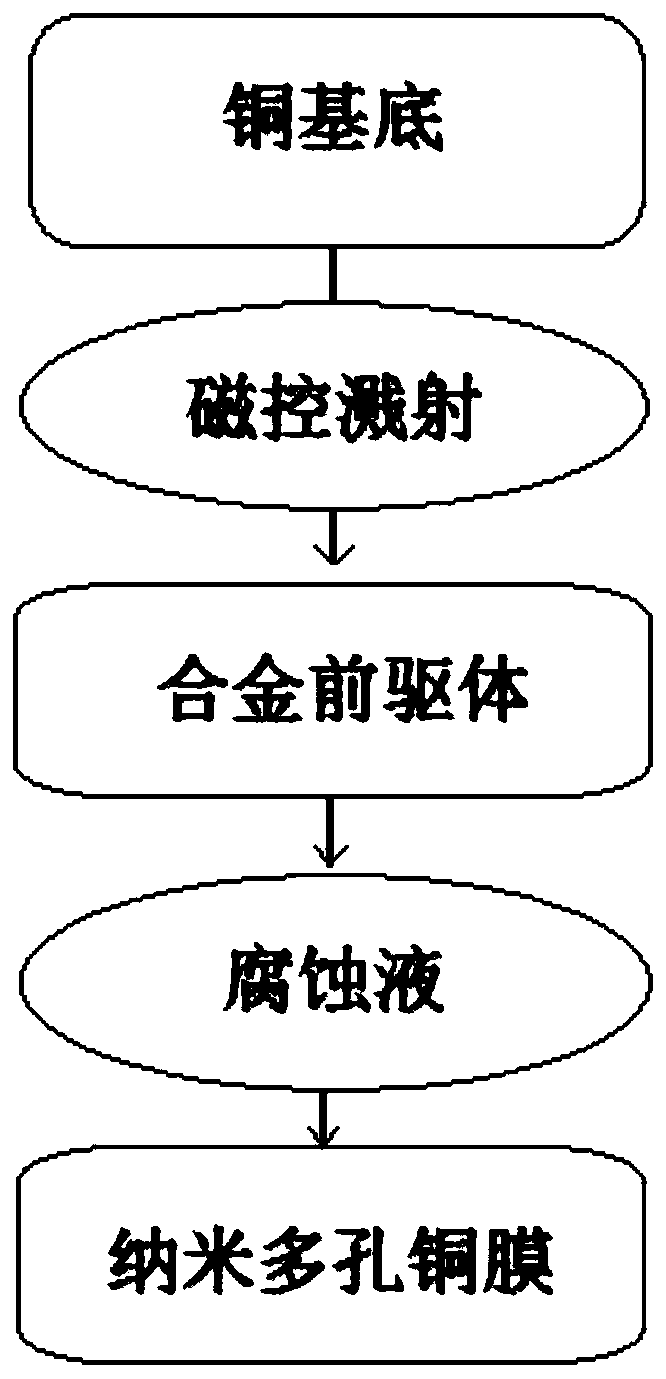
[0029] The invention provides a method for preparing a high-purity nanoporous copper film, which is specifically implemented according to the following steps, and the preparation flow chart is as follows figure 1 Shown:
[0030] A method for preparing a high-purity nanoporous copper film, characterized in that it is specifically implemented according to the following steps:
[0031] Step 1, cutting the copper substrate;
[0032] Step 2, cleaning the copper substrate obtained in step 1;
[0033] Fix the copper substrate cut in step 1 on the sample base of the magnetron sputtering apparatus, fix the pure copper target and the pure aluminum target on the target position, and then rotate the baffle to the middle of the target platform and the target position , close the chamber door to make the vacuum chamber sealed, open the argon gas flow valve after vacuuming, let in argon gas to increase the pressure in the vacuum chamber, adjust the bias voltage of the copper substrate, and...
Embodiment 1
[0045] This embodiment discloses a method for preparing a high-purity nanoporous copper film, which is specifically implemented according to the following steps:
[0046] The base copper sheet used in the experiment is a single-sided polished copper sheet with a diameter of 100±0.5mm and a thickness of 500±15μm.
[0047] Step 1, cutting the copper sheet; cutting the purchased silicon wafer with a diamond knife or a laser, and cutting it into several square specifications of 10×10mm;
[0048] Step 2, cleaning the copper substrate obtained in step 1;
[0049] Fix the copper substrate cut in step 1 on the sample base of MSIP016 magnetron sputtering equipment, turn on the mechanical pump and pre-evacuate to 4×10 -3 After Pa, open the argon gas flow valve, pass in argon gas, make the pressure in the vacuum chamber reach 0.1Pa, then adjust the substrate bias voltage to 350V, set the sputtering current of the copper target to 0.2A, and the sputtering voltage to 300V. The sputtering...
Embodiment 2
[0059] This embodiment discloses a method for preparing a high-purity nanoporous copper film, which is specifically implemented according to the following steps:
[0060] The base copper sheet used in the experiment is a single-sided polished copper sheet with a diameter of 100±0.5mm and a thickness of 500±15μm.
[0061] Step 1, cutting the copper sheet; cutting the purchased silicon wafer with a diamond knife or a laser, and cutting it into several square specifications of 10×10mm;
[0062] Step 2, cleaning the copper substrate obtained in step 1;
[0063] Fix the copper substrate cut in step 1 on the sample base, turn on the mechanical pump and pre-evacuate to 4×10 -3 After Pa, open the argon gas flow valve, pass in argon gas, make the pressure in the vacuum chamber reach 0.1Pa, then adjust the substrate bias voltage to 350V, set the sputtering current of the copper target to 0.2A, and the sputtering voltage to 300V. The sputtering current of the target is 0.3A, the sputte...
PUM
| Property | Measurement | Unit |
|---|---|---|
| Thickness | aaaaa | aaaaa |
Abstract
Description
Claims
Application Information


