Image sensing unit and manufacturing method thereof, and image sensor

A sensor unit and image technology, applied in radiation control devices and other directions, can solve the problems of excessively thick device layer processing difficulty, reduced incident photon absorption efficiency, and large incident light angle, so as to overcome low light absorption efficiency and improve light Absorption efficiency, the effect of prolonging the effective optical path

Pending Publication Date: 2019-05-24
SHENZHEN ADAPS PHOTONICS TECH CO LTD
View PDF0 Cites 5 Cited by
  • Summary
  • Abstract
  • Description
  • Claims
  • Application Information

AI Technical Summary

Problems solved by technology

However, an overly thick device layer requires a corresponding increase in the area of ​​the image sensor, which reduces the number of units per unit area, and the processing of an overly thick device layer is difficult, the yield is low, and it is not easy to be compatible with the CMOS process, which increases the cost.
[0006] (2) Increase the incident rate of light by adding an anti-reflection film on the surface of the image sensor's planar structure, but its anti-reflection effect will decrease with the increase of the incident angle, resulting in a decrease in the absorption efficiency of incident photons
[0007] (3) For the image sensing unit array, the units located at the edge of the array receive a larger angle of incident light converged by the lens, which may lead to a reduction in absorption efficiency
However, there are many disadvantages in this method: 1) when the actual processing thickness of the silicon layer deviates slightly from the design, the resonance frequency will shift; 2) it is very sensitive to the wavelength of the incident light, and the absorption efficiency of light that deviates from the resonance frequency 3) When the temperature changes, the resonant frequency will also shift due to the slight change in the refractive index of the material; 4) It is very sensitive to the change of the incident light angle

Method used


Image

  • Image sensing unit and manufacturing method thereof, and image sensor
  • Image sensing unit and manufacturing method thereof, and image sensor
  • Image sensing unit and manufacturing method thereof, and image sensor

Examples


Embodiment 1

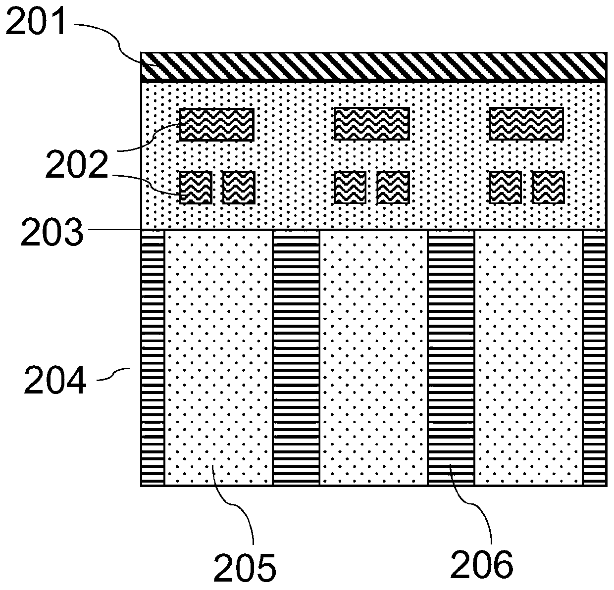
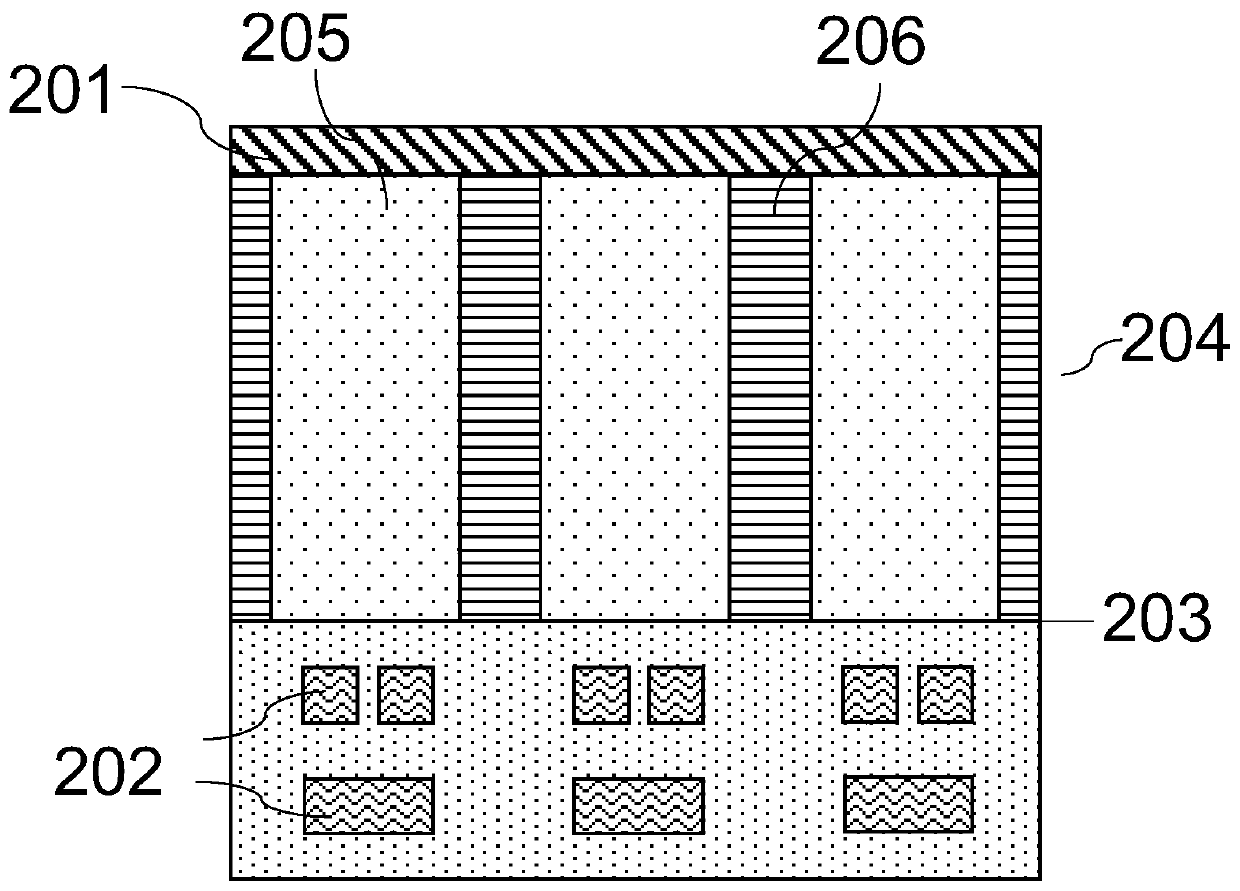
[0055] An image sensing unit. The image sensing unit is sequentially provided with a substrate, a circuit layer, a silicon oxide layer and a silicon detection layer from bottom to top. The silicon detection layer is surrounded by sidewall reflective walls, and the image sensing unit is provided with Light trapping structure. Furthermore, the upper surface of the image sensing unit is also provided with an anti-reflection structure.

[0056] Since the image sensing unit is equipped with a light trapping structure, the incident light is scattered to various angles after being reflected, scattered, and refracted by the light trapping structure. Together with the reflection effect of the side wall reflecting wall, the light in the image sensing unit can be extended. The effective optical length can significantly improve the absorption efficiency of near-infrared light without increasing the thickness of the silicon layer, and overcome the technical problem of low light absorption eff...

Embodiment 2

[0058] Based on the further improvement of embodiment 1, embodiment 2 is obtained. The light trapping structure is arranged on the upper surface of the image sensor unit and / or above the silicon oxide layer and / or below the silicon oxide layer, and the image sensor unit is separately arranged on the upper surface. The light trapping structure, the light trapping structure above the silicon oxide layer, or the light trapping structure below the silicon oxide layer can all improve the light absorption efficiency, and can also be used in combination. Further, the light-trapping structure is a nano-scale or micro-level uneven structure, for example, the light-trapping structure may be an inverted pyramid structure 1 (reference Figure 4 ) Or shallow trench structure 13 (e.g. Picture 10 As shown, the shallow groove structure 13 is provided on the upper surface of the image sensing unit), or the surface is a honeycomb surface, a sinusoidal grating textured surface, a dimple-like order...

Embodiment 3

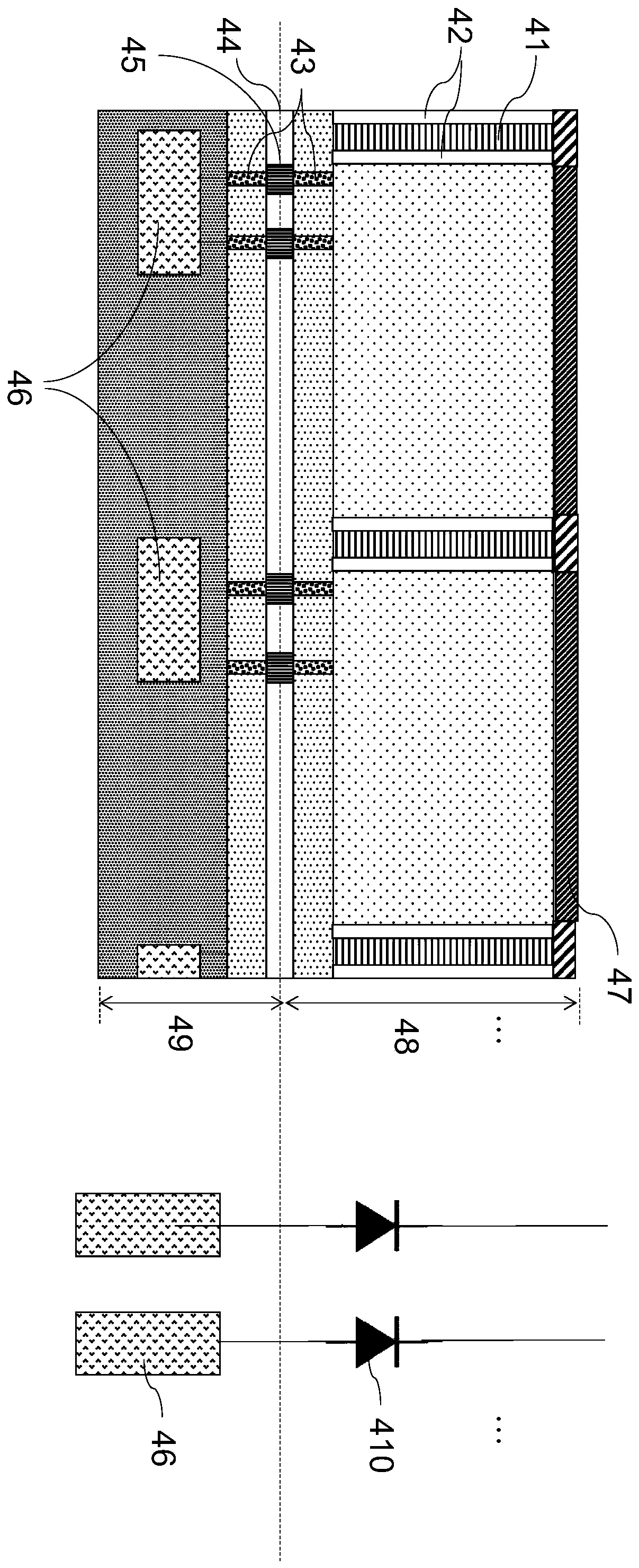
[0062] Example 3 is obtained based on the further improvement of Example 1. Refer to Figure 8 , Figure 8 It is a schematic diagram of the cross-sectional structure of the third embodiment of an image sensing unit in the present invention; the light trapping structure and / or the antireflection structure is an inverted pyramid structure 1, and the inverted pyramid structure 1 has both light trapping and antireflection functions, specifically The inverted pyramid structure 1 is arranged on the upper surface of the image sensing unit (that is, arranged above the silicon detection layer 6), and the inverted pyramid structure 1 is obtained by filling silicon oxide after etching on a silicon substrate. In this embodiment, an insulating dielectric protective layer 5 is provided above the inverted pyramid structure 1 to protect the image sensor unit. Specifically, the inverted pyramid structure 1 arranged on the upper surface of the image sensing unit can form a gently gradual change i...


PUM


Abstract

The invention discloses an image sensing unit and a manufacturing method thereof, and an image sensor. The image sensing unit is provided with light trapping structures. The incident light is dispersed to various angles after being reflected, scattered and refracted by the light trapping structure, which, with the addition of the reflection function of a sidewall reflecting wall, can extend the effective optical path of the light in the image sensing unit. Therefore, the absorption efficiency of light in the image sensing unit can be improved without increasing the thickness of the device. Inaddition, a manufacturing method of the image sensing unit is disclosed, which realizes the manufacture of the image sensing unit. The image sensing unit has a first light trapping structure and a second light trapping structure, which can improve the light absorption efficiency of the image sensing unit.

Description

Technical field [0001] The invention relates to the field of optoelectronics, in particular to an image sensor unit, a manufacturing method thereof, and an image sensor. Background technique [0002] Image sensors are widely used in various electronic devices, such as digital cameras, mobile phones, medical imaging equipment, security inspection equipment, rangefinder cameras and so on. With the continuous advancement of semiconductor technology for manufacturing image sensors, image sensors are further developing towards low power consumption, miniaturization, and high integration. The image sensor is usually composed of a photodetector array. The image sensor unit can be a traditional CMOS image sensing unit (CIS) or a single photon avalanche diode (SPAD), both of which can be integrated and manufactured through a CMOS process. In addition, the image sensor includes a front-illuminated image sensor and a back-illuminated image sensor. The cross-sectional structure diagram of t...

Claims


Application Information

Patent Timeline
Patent Type & Authority Applications(China)
IPC IPC(8): H01L27/146
Inventor 臧凯李爽马志洁
Owner SHENZHEN ADAPS PHOTONICS TECH CO LTD
Why Eureka
Try Eureka