Perovskite photoelectric detector with optical micro cavity structure and preparation method thereof

A photoelectric detector and optical microcavity technology, which is applied in the field of visible light detection, can solve the problems of poor detection performance and wide half-wave peak of the detector, and achieve the effect of novel and unique structure, narrow detection half-wave peak width, and improve device performance

Inactive Publication Date: 2019-06-04
UNIV OF ELECTRONICS SCI & TECH OF CHINA
View PDF4 Cites 15 Cited by
  • Summary
  • Abstract
  • Description
  • Claims
  • Application Information

AI Technical Summary

Problems solved by technology

However, the half-peak width of the existing perovskite photodetectors is wide, which makes the detection performance of the detectors poor.

Method used


Image

  • Perovskite photoelectric detector with optical micro cavity structure and preparation method thereof
  • Perovskite photoelectric detector with optical micro cavity structure and preparation method thereof
  • Perovskite photoelectric detector with optical micro cavity structure and preparation method thereof

Examples


Embodiment 1

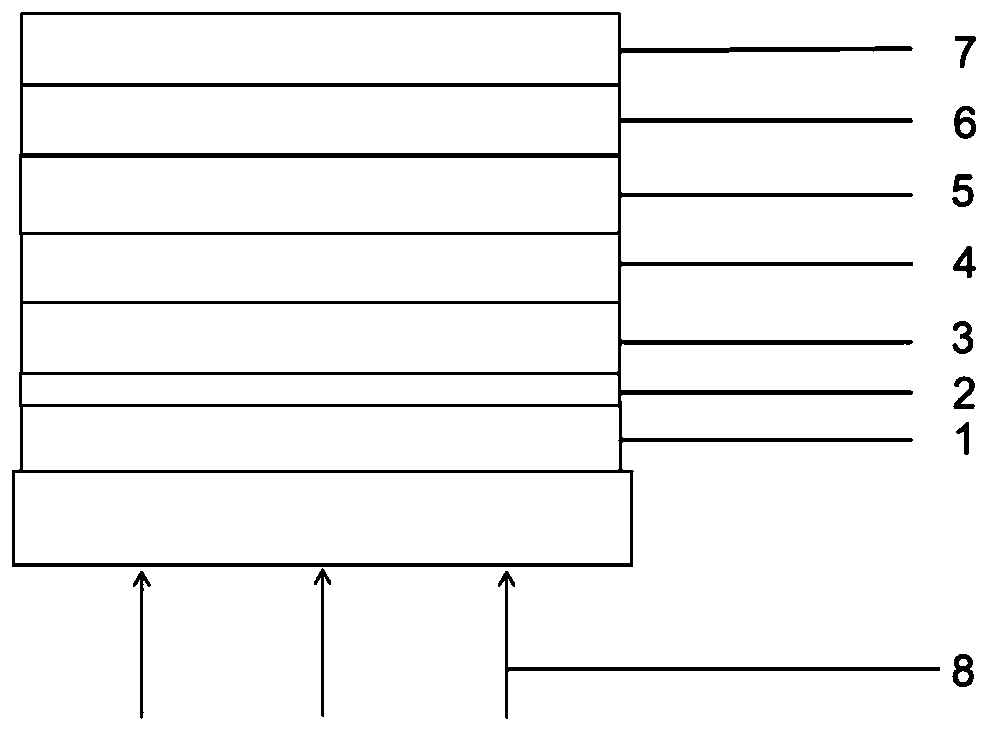
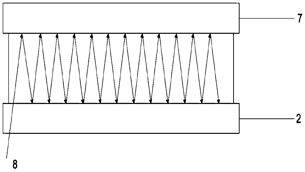
[0040] A perovskite photodetector with an optical microcavity structure based on the charge-narrowing absorption effect, such as figure 1 As shown, including bottom-up glass substrate, transparent conductive electrode layer 1, light reflection layer 2, hole transport layer 3, perovskite sensitive layer 4, electron transport layer 5, hole blocking layer 6 and metal electrode layer 7. Among them, the transparent conductive electrode layer 1 adopts an ITO transparent conductive electrode with a thickness of 150nm, the light reflection layer 2 adopts silver with a thickness of 5nm, and the hole transport layer 3 adopts PEDOT:PSS film, CuSCN, CuI, NiO with a thickness of 90nm. x In any one, the perovskite sensitive layer 4 adopts CH with a thickness of 500nm 3 NH 3 PB 2 Br film, the electron transport layer 5 adopts PC with a thickness of 80nm 61 BM film, TiO 2 And any one of ZnO, the hole transport layer 3 adopts C with a thickness of 80nm 60 Thin film, ZnO, BCP and Al 2 o ...

Embodiment 2

[0053] On the basis of Example 1, methylamine lead bromine was dissolved in DMF (N-N dimethylformamide) solution, and after stirring for 6 hours at 100°C, a perovskite precursor solution was obtained; the light reflection layer was 2nm thick Gold; the thickness of the perovskite sensitive layer 4 is 50nm;

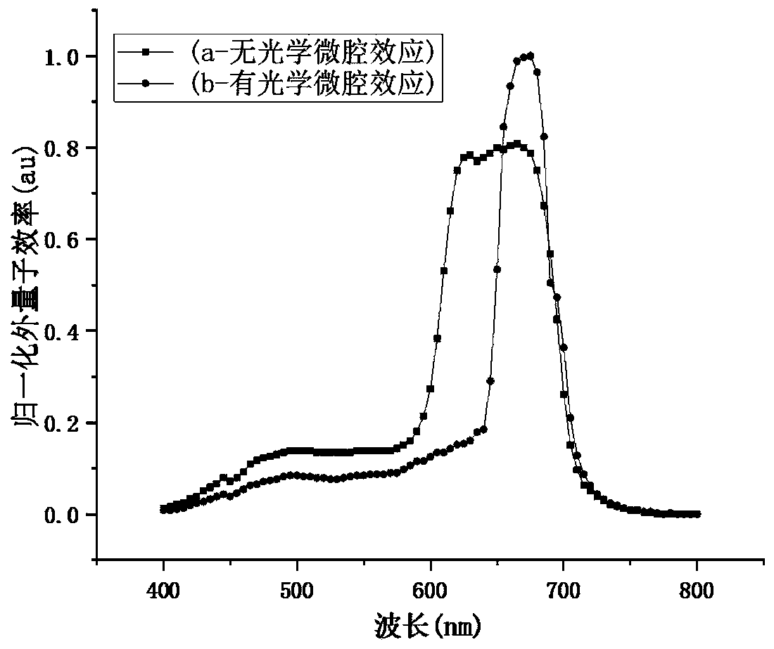
[0054] Under standard test conditions, a light beam is extracted from a visible light source, so that the incident light 8 is vertically incident on the perovskite photodetector. The test results show that the perovskite visible light detector responds to the 525-575nm band, and its half-wave peak width is 40nm at the peak of 550nm, and its detection rate is ~10 12 Jones.

Embodiment 3

[0056] On the basis of Example 1, methylamine lead iodide and methylamine lead bromine are dissolved in DMF (N-N dimethylformamide) solution according to the molar ratio of 1.4:0.6, and doped with PEIE of 0.33% mass ratio, in After stirring at 100° C. for 6 hours, a perovskite precursor solution was obtained; the light reflection layer was made of aluminum with a thickness of 10 nm; the thickness of the perovskite sensitive layer 4 was 5000 nm;

[0057] Under standard test conditions, a light beam is extracted from a visible light source, so that the incident light 8 is vertically incident on the perovskite photodetector. The test results show that the perovskite visible light detector responds to the 400-500nm band, and its half-wave peak width is 50nm at the peak of 450nm, and its detection rate is ~10 12 Jones.


PUM


Abstract

The invention belongs to the technical field of visible light detection, and specifically discloses a perovskite photoelectric detector with an optical micro cavity structure and a preparation methodthereof. The perovskite photoelectric detector comprises a glass substrate, a transparent conductive electrode layer, a light reflection layer, a hole transport layer, a perovskite sensitive layer, anelectron transport layer, a hole barrier layer and a metal electrode layer arranged in turn from bottom to top. The perovskite sensitive layer comprises multiple materials selected from a typical halogen perovskite material with a chemical formula of ABX<3>, a monovalent cation substituted perovskite material with a chemical formula of A<x><1>A<1-x><2>BM (0<x<1), a halogen substituted solid solution perovskite material with a chemical formula of ABM<x><1>M<3-x><2> (0<x<3), a metal substituted solid solution perovskite material with a chemical formula of AB<x><1>B<1-x><2>M (0<x<1) and a two-dimensional perovskite material. The thickness of the perovskite sensitive layer is 50-5000nm. By arranging the perovskite sensitive layer materials and making the perovskite film thick, a charge narrowing absorption effect is achieved, the detection half-wave peak width of the detector can be narrowed, and the detection performance of the detector can be improved.

Description

technical field [0001] The invention belongs to the technical field of visible light detection, in particular to a perovskite photodetector with an optical microcavity structure and a preparation method thereof. Background technique [0002] A photodetector is a device that detects and measures the properties of light through the photoelectric effect, usually manifested as a photocurrent. With the rapid development of modern science and technology and the continuous expansion of application fields, photoelectric detection technology has very important practical significance in various fields such as production, scientific research, military affairs, and optoelectronics. Photodetectors from the ultraviolet-visible light region to the infrared light region have a wide range of applications in the fields of industry, science and technology. For example, detectors in the ultraviolet region can be used for ultraviolet guidance, detection of cancer cells, observation of earthquak...

Claims


Application Information

Patent Timeline
Patent Type & Authority Applications(China)
IPC IPC(8): H01L51/42H01L51/44H01L51/46H01L51/48
CPCY02E10/549
Inventor 张磊黄江宛晨侯思辉
Owner UNIV OF ELECTRONICS SCI & TECH OF CHINA
Why Eureka
Try Eureka