

Test method for measuring metal of silicon wafer body
A test method and technology of silicon wafers, applied in the direction of semiconductor/solid-state device testing/measurement, etc., can solve the problems of roughness effect, high cost, balance volume effect, etc., to achieve accurate test results, reduce test costs, and low size requirements. Effect
- Summary
- Abstract
- Description
- Claims
- Application Information
AI Technical Summary
Problems solved by technology
Method used
Image

Examples
Embodiment Construction
[0024] It should be noted that, in the case of no conflict, the embodiments of the present invention and the features in the embodiments can be combined with each other.
[0025] In describing the present invention, it should be understood that the terms "center", "longitudinal", "transverse", "upper", "lower", "front", "rear", "left", "right", " The orientations or positional relationships indicated by "vertical", "horizontal", "top", "bottom", "inner", "outer", etc. are relative orientations or positional relationships, which are only for the convenience of describing the present invention and simplifying the description, rather than Nothing indicating or implying that a referenced device or element must have a particular orientation, be constructed, and operate in a particular orientation should therefore not be construed as limiting the invention. In addition, the terms "first", "second", etc. are used for descriptive purposes only, and should not be understood as indicati...
PUM
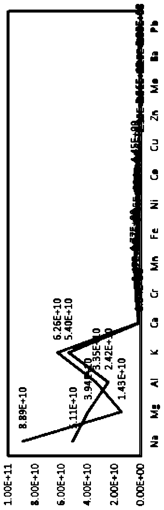
| Property | Measurement | Unit |
|---|---|---|
| electrical resistivity | aaaaa | aaaaa |
Abstract
Description
Claims
Application Information