Quantum dot photoelectric detector based on atomic layer deposition and preparation method thereof

A photodetector, atomic layer deposition technology, applied in photovoltaic power generation, electric solid state device, semiconductor/solid state device manufacturing, etc. Slow device response speed and other problems, to achieve the effect of increasing life and mobility, reducing dark current, and improving the ratio of light to dark current

Active Publication Date: 2019-06-21
HUAZHONG UNIV OF SCI & TECH
View PDF3 Cites 2 Cited by
  • Summary
  • Abstract
  • Description
  • Claims
  • Application Information

AI Technical Summary

Problems solved by technology

However, the photodetector prepared by this method has a large dark current and a small photocurrent. After the ligand exchange, the quantum dot photodetector has the disadvantages of low photo-dark current ratio and slow response time, and the device performance is very poor.
[0004] In order to solve the shortcomings of poor performance of single-layer films, metal nanocrystals such as Ag or Au are doped into the quantum dot film, which prolongs the lifetime of photon carriers and improves the photocurrent of the device, but the introduced traps will slow down the response of the device. speed, the dark current of the device will also increase accordingly, and the introduction of noble metal nanocrystals will also greatly increase the manufacturing cost, which is not suitable for the mass production of quantum dot photodetectors

Method used


Image

  • Quantum dot photoelectric detector based on atomic layer deposition and preparation method thereof
  • Quantum dot photoelectric detector based on atomic layer deposition and preparation method thereof
  • Quantum dot photoelectric detector based on atomic layer deposition and preparation method thereof

Examples


preparation example Construction

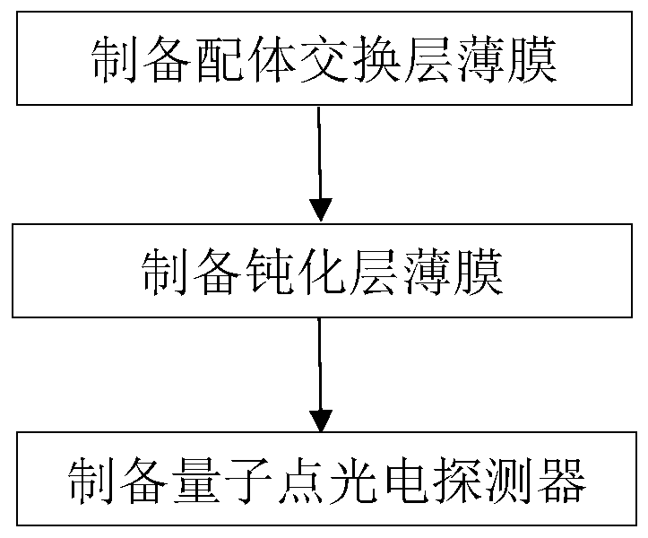
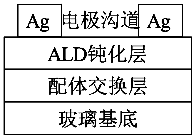
[0029] Such as figure 1 Shown, the present invention proposes a kind of preparation method based on the quantum dot photodetector of atomic layer deposition, and this method comprises the steps:

[0030] (a) Set the rotation speed of the spin coater at 1500rpm to 3000rpm, and the acceleration at 15m / s 2 ~30m / s 2 , the quantum dot solution is spin-coated on a clean substrate with a spin coater to obtain a single-layer quantum dot film with a thickness of 10nm to 50nm, and the first quantum dot is obtained by controlling the number of cycles of the spin coater to be 1 to 10 times film, the first quantum dot film is composed of 1-10 layers of single-layer quantum dot film, the thickness of the single-layer quantum dot film is preferably 10nm-50nm, and then the organic ligand solution is drip-coated on the first quantum dot Put it on the film and let it stand for 10s ~ 100s, after the ligand exchange is completed, wash it with a solvent such as methanol, acetonitrile or hexane, ...

Embodiment 1

[0044] (a) Configure a PbS solution with a concentration of 50mg / mL as the quantum dot solution, set the spin coater’s speed at 1500rpm, and the acceleration at 15m / s 2 , Spin-coat the PbS solution on a clean substrate with a spin coater to obtain a single-layer quantum dot film with a thickness of 50nm, cycle once to obtain the first quantum dot film, and then use the TBAI solution with a concentration of 1mg / mL as the organic compound The body solution is dripped on the first quantum dot film for 20s and left to stand for 10s, and after the ligand exchange is completed, it is washed with methanol, thereby completing the preparation of the ligand exchange layer film;

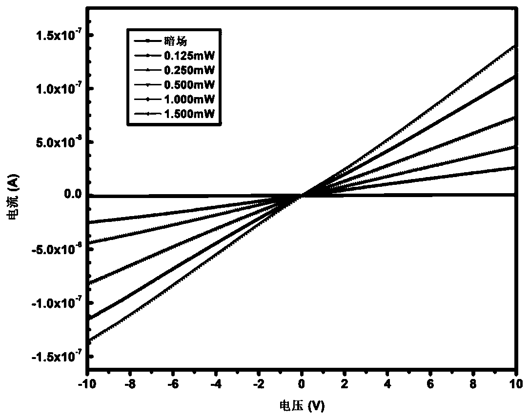
[0045] (b) Set the rotational speed of the spin coater to 1500rpm and the acceleration to 15m / s 2 , using a spin coater to spin-coat the PbS solution with a concentration of 5 mg / mL on the ligand exchange layer film to prepare a single-layer quantum dot film with a thickness of 50 nm, and then in the vacuum cha...

Embodiment 2

[0047] (a) Configure the PbSe solution with a concentration of 5mg / mL as the quantum dot solution, set the spin coating apparatus to rotate at 3000rpm, and accelerate at 30m / s 2 , Spin-coat the PbSe solution on a clean substrate with a spin coater to obtain a single-layer quantum dot film with a thickness of 10nm, cycle 10 times to obtain the first quantum dot film, and then use a CTAB solution with a concentration of 100mg / mL as the organic compound The body solution is dripped on the first quantum dot film for 60s and left to stand for 80s, and after the ligand exchange is completed, it is washed with methanol, thereby completing the preparation of the ligand exchange layer film;

[0048] (b) Set the rotational speed of the spin coater to 3000rpm and the acceleration to 30m / s 2 , using a spin coater to spin-coat the PbSe solution with a concentration of 50 mg / mL on the ligand exchange layer film to prepare a single-layer quantum dot film with a thickness of 10 nm, and then i...


PUM


Abstract

The invention belongs to the preparation field of the optical material, and discloses a quantum dot photoelectric detector based on atomic layer deposition, and a preparation method thereof. The preparation method comprises the following steps: spinning-coating a quantum dot solution on a clean substrate to prepare a first quantum dot thin film, and then dropping an organic matter ligand solutionon the first quantum doe thin film to cover the same, and standing for a certain time, cleaning by using a solvent after the ligand exchange is accomplished, thereby accomplishing the preparation of the ligand exchange layer thin film; spinning-coating the quantum dot solution on the ligand exchange layer thin film to prepare a monolayer quantum dot thin film; performing atomic layer deposition oninert atmosphere so as to sufficiently passivate the monolayer quantum dot thin film, repeating the above steps so as to acquire a passivation layer thin film; and evaporating electrode on the passivation layer thin film to manufacture the quantum dot photoelectric detector. The quantum dot thin film surface is passivated by adopting the atomic layer deposition technology, the light and dark current ratio of the device can be improved, the device performance of the detector is optimized, and a PN-junction dual-layer structure is formed, and the response speed can be effectively improved.

Description

technical field [0001] The invention belongs to the field of optical material preparation, and more specifically relates to a quantum dot photodetector based on atomic layer deposition and a preparation method thereof. Background technique [0002] Quantum dots, also known as nanocrystals, are nanoparticles composed of II-VI or III-V elements. The particle size of quantum dots is generally between 1nm and 10nm. Since electrons and holes are quantum-confined, the continuous energy band structure becomes a discrete energy level structure with molecular characteristics, which can emit fluorescence after being excited. The emission spectrum of quantum dots can be controlled by changing the size of the quantum dots. It has good photostability, wide excitation spectrum and narrow emission spectrum. It has a wide range of applications in the fields of solar cells, light-emitting devices, and optical biomarkers. application prospects. [0003] At present, in the field of quantum d...

Claims


Application Information

Patent Timeline
Patent Type & Authority Applications(China)
IPC IPC(8): H01L51/48H01L51/42H01L51/44B82Y40/00
CPCY02E10/549
Inventor 陈蓉姜晨晨单斌曹坤文艳伟周彬泽向勤勇耿士才井尧刘梦佳
Owner HUAZHONG UNIV OF SCI & TECH
Why Eureka
Try Eureka