An energy-saving and environment-friendly organic light-emitting element
An organic light-emitting element, energy-saving and environmentally friendly technology, applied in electrical components, semiconductor devices, electro-solid devices, etc., can solve the problem of not being able to optimize electronic conduction loss and organic interface loss at the same time.
- Summary
- Abstract
- Description
- Claims
- Application Information
AI Technical Summary
Problems solved by technology
Method used
Image
Examples
Embodiment 1
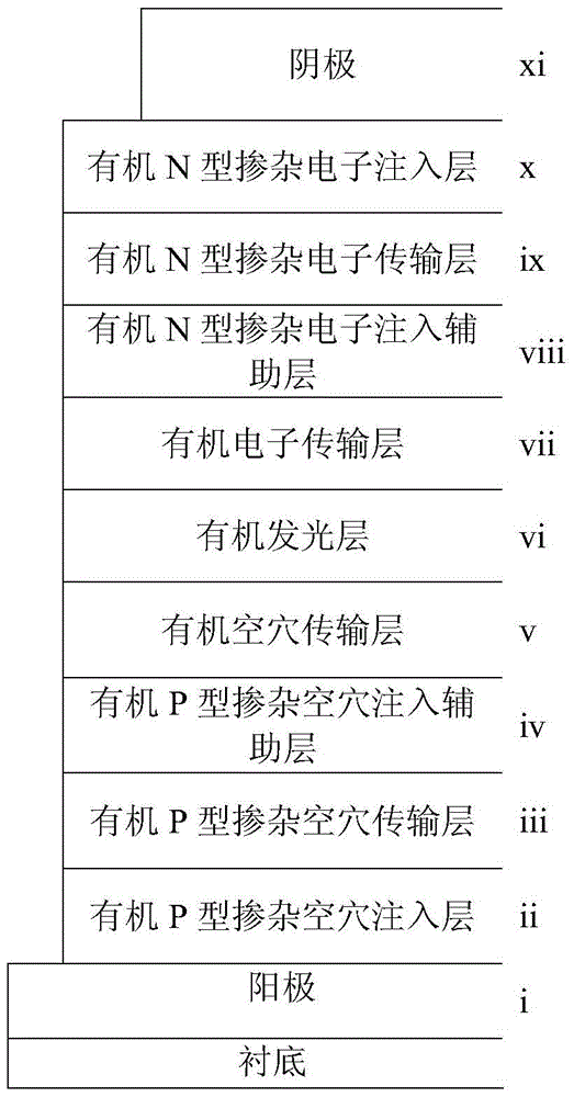
[0059] The preparation structure is ITO / CBP:ReO 3 =1:0.01 Thickness 1nm / m-MTDATA:F 4 TCNQ=1:0.01 Thickness 10nm / CBP:ReO 3 =1:0.01 Thickness 1nm / CBP Thickness 10nm / Alq3 Thickness 60nm / Bphen Thickness 5nm / Bphen:Cs=1:0.01 Thickness 5nm / NTCDA:LCV=1:0.01 Thickness 20nm / Bphen:Cs=1:0.01 Thickness 5nm / Al Organic light-emitting diodes with a thickness of 100nm.
[0060] The organic light-emitting diode is composed of a layer of ITO anode on a glass substrate, a layer of CBP:ReO with a thickness of 1 nm deposited on the ITO anode. 3 Thin film organic P-type doped hole injection layer, one layer deposited on CBP:ReO 3 m-MTDATA with a thickness of 10 nm on the thin-film organic P-type doped hole-injection layer: F 4 TCNQ thin film organic P-type doped hole transport layer, one layer deposited on m-MTDATA:F 4 1nm-thick CBP:ReO on TCNQ thin-film organic P-type doped hole-transport layer 3Thin film organic P-type doped hole injection auxiliary layer, one layer deposited on CBP:ReO 3 A...
Embodiment 2
[0101] The preparation structure is ITO / TCTA: MoO 3 =1:1 thickness 20nm / MeO-TPD:ReO 3 =1:1 thickness 200nm / TCTA:MoO 3 =1:1 thickness 20nm / TCTA thickness 50nm / Alq3 thickness 60nm / Bphen thickness 20nm / Bphen:Cs=1:0.5 thickness 20nm / NTCDA:LCV=1:0.1 thickness 300nm / Bphen:Cs=1:0.5 thickness 20nm / Al Organic light-emitting diodes with a thickness of 100nm.
[0102] The organic light-emitting diode is composed of a layer of ITO anode on a glass substrate, a layer of TCTA: MoO deposited on the ITO anode with a thickness of 20nm 3 Thin film organic P-type doped hole injection layer, one layer deposited on TCTA: MoO 3 MeO-TPD:ReO with a thickness of 200 nm on a thin-film organic P-type doped hole-injection layer 3 Thin-film organic P-type doped hole transport layer, one layer deposited on MeO-TPD: ReO 3 20 nm thick TCTA:MoO on thin-film organic P-type doped hole-transport layer 3 Thin film organic P-type doped hole injection auxiliary layer, one layer deposited on TCTA: MoO 3 TCTA ...
Embodiment 3
[0130] The prepared structure is Au 20nm / CBP:ReO 3 =1:0.01 Thickness 1nm / m-MTDATA:F 4 TCNQ=1:0.01 Thickness 10nm / CBP:ReO 3 =1:0.01 Thickness 1nm / CBP Thickness 10nm / Alq3 Thickness 60nm / Bphen Thickness 5nm / Bphen:Cs=1:0.01 Thickness 5nm / NTCDA:LCV=1:0.01 Thickness 20nm / Bphen:Cs=1:0.01 Thickness 5nm / Al Organic light-emitting diodes with a thickness of 100nm.
[0131] The organic light-emitting diode is composed of a layer of Au anode with a thickness of 20 nm on a glass substrate, a layer of CBP:ReO with a thickness of 1 nm deposited on the Au anode 3 Thin film organic P-type doped hole injection layer, one layer deposited on CBP:ReO 3 m-MTDATA with a thickness of 10 nm on the thin-film organic P-type doped hole-injection layer: F 4 TCNQ thin film organic P-type doped hole transport layer, one layer deposited on m-MTDATA:F 4 1nm-thick CBP:ReO on TCNQ thin-film organic P-type doped hole-transport layer 3 Thin film organic P-type doped hole injection auxiliary layer, one layer ...
PUM
 Abstract
Description
Claims
Application Information


