Semiconductor carrier type judgment and band gap measurement method

A technology of forbidden band width and measurement method, which is applied in the field of semiconductor material detection, can solve the problems of tedious normalization process of photoconductive method, difficulty in accurately measuring forbidden band width, adult human error, etc., and achieves remarkable application effect.

Inactive Publication Date: 2019-06-25
FUJIAN NORMAL UNIV
View PDF4 Cites 3 Cited by
  • Summary
  • Abstract
  • Description
  • Claims
  • Application Information

AI Technical Summary

Problems solved by technology

Among them, the optical absorption coefficient method is first based on the optical method to measure the absorption coefficient α of the semiconductor thin film, and then do (αhν) by the Tauc method n The linear part of the -(hν) curve intercepts the horizontal axis, and there is a large human error; the photoconductivity method needs a tedious normalization process during the test; and the photoluminescence spectroscopy often only qualitatively compares the samples. Bandgap width
Not only that, all the above measurement methods are susceptible to factors such as exciton absorption or exciton emission, absorption or radiative recombination between the intrinsic band and shallow impurities, which brings difficulties to accurately measure the forbidden band width

Method used


Image

  • Semiconductor carrier type judgment and band gap measurement method
  • Semiconductor carrier type judgment and band gap measurement method
  • Semiconductor carrier type judgment and band gap measurement method

Examples


Embodiment 1

[0057] The present invention will be described below by taking the measurement of the forbidden band width of CuO thin film semiconductor material as an example. The specific steps are as follows:

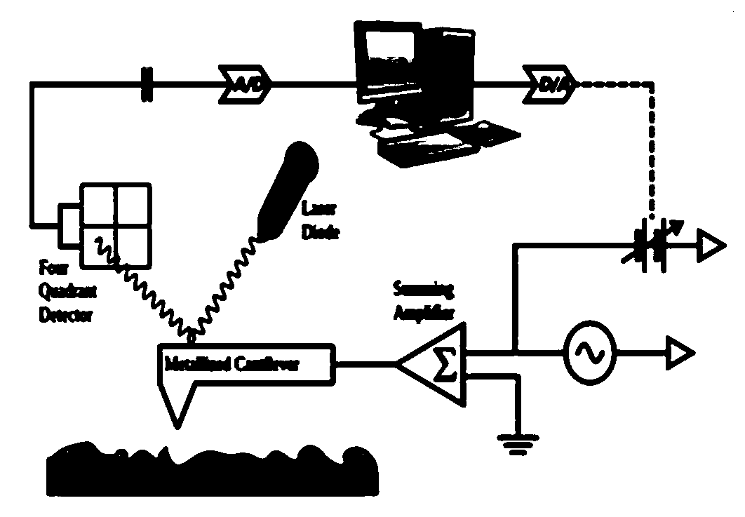
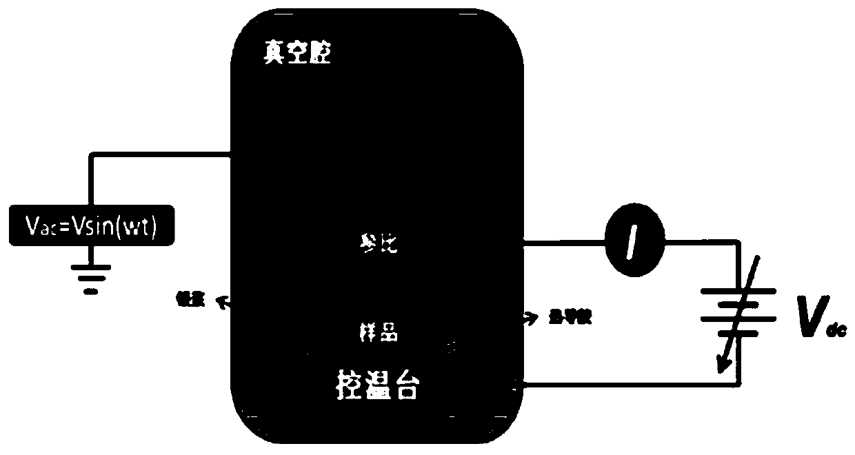
[0058] S 1 : The CuO thin film semiconductor material is fixed on the copper heating stage with thermal conductive glue, and its surface is bonded and conducted with the sample stage with silver paste. Evacuate the vacuum test chamber equipped with a Kelvin probe to 6.0×10 -4 Pa to isolate the heat transfer from the heating stage to the Kelvin reference probe. At the same time, the work function 5.30eV at the temperature of 298K of the material was measured and recorded.

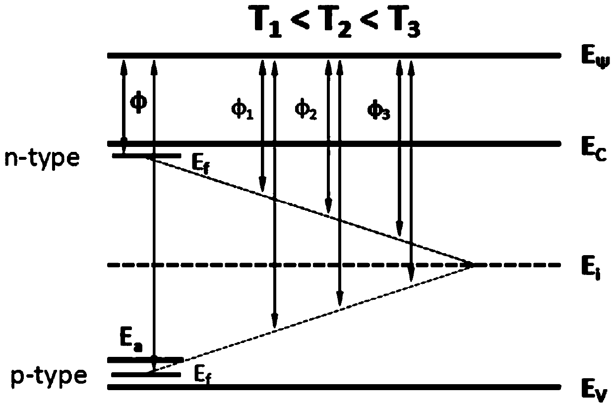
[0059] S 2 : The sample is heated to cause thermal excitation of the material, and the work function measurement is performed every 5K at the same time. The measurement results show that the work function of the material decreases with the increase of temperature, that is, the Fermi energy level of the mater...

Embodiment 2

[0063] Taking the zero-bandgap lead-palladium-oxygen P-type semiconductor thin film as the research object, using the same test steps as in Example 1, the measured Fermi level changes show the characteristics of hole carriers, and the band gap is 0.34eV, which is consistent with the literature report. similar.

Embodiment 3

[0065] Taking N-type single crystal silicon as the research object, using the same test steps as in Example 1, the test results show that the Fermi level decreases with the increase of temperature, the material presents N-type semiconductor characteristics, and the band gap is 1.23eV, the test results more precise.

[0066] The present invention adopts the above technical scheme, utilizes the change law of extrinsic semiconductor Fermi energy level with temperature at different temperatures to analyze the carrier type and forbidden band width of the material, effectively prevent exciton absorption or exciton emission, and the intrinsic band Influenced by factors such as absorption or radiation recombination with shallow impurities; the test calculation scheme is based on semiconductor energy band theory and high-precision experimental measurement methods, which can effectively improve the measurement accuracy of the bandgap width of extrinsic semiconductor materials and simplif...


PUM

PropertyMeasurementUnit
thicknessaaaaaaaaaa

Abstract

The invention discloses a semiconductor carrier type judgment and band gap measurement method. A Kelvin probe method is used to measure a work function of an extrinsic semiconductor material at different temperatures, the change law of a Fermi level of the material along with temperature is determined, and the carrier type is judged; and on the basis, in combination of the relationship of the extrinsic semiconductor material work function along with temperature changes, the change relationship between the Fermi level caused by electron thermal excitation and the relative position of a conduction band and a valence band is analyzed, and the band gap is solved. The measurement method disclosed in the invention is based on a semiconductor energy band theory, compared with the conventional optical band gap measurement method, the method of the invention can measure the band gap of a non-transmissive semiconductor material while the accuracy is greatly improved.

Description

technical field [0001] The invention relates to the technical field of semiconductor material detection, in particular to a method for judging the type of semiconductor carriers and measuring the forbidden band width. Background technique [0002] The development of semiconductor materials is the basis and premise to promote the progress of semiconductor science and technology. The forbidden band width is an important characteristic parameter that determines the conductivity of semiconductors. The determination of this parameter is of great significance in the study of the crystal structure and energy band structure of semiconductor materials. [0003] There are many methods for measuring and characterizing the bandgap of semiconductor materials, such as optical absorption coefficient method, photoconductivity method and photoluminescence spectroscopy. Among them, the optical absorption coefficient method is first based on the optical method to measure the absorption coeff...

Claims


Application Information

Patent Timeline
Patent Type & Authority Applications(China)
IPC IPC(8): G01N21/71
Inventor 陈越黄志高林应斌
Owner FUJIAN NORMAL UNIV
Why Eureka
Try Eureka