Microchannel-nanoporous composite structure evaporator of substrate level of GaN HEMT device
A nanoporous, composite structure technology, applied in the direction of electrical solid devices, semiconductor devices, semiconductor/solid device components, etc., can solve problems such as high heat flux density, achieve uniform temperature distribution, reduce temperature, and reduce pump power consumption Effect
- Summary
- Abstract
- Description
- Claims
- Application Information
AI Technical Summary
Problems solved by technology
Method used
Image
Examples
Embodiment 1
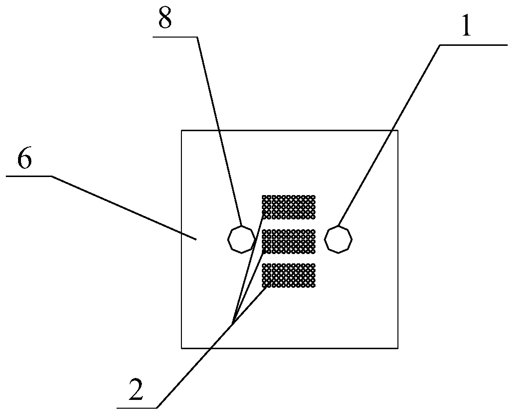
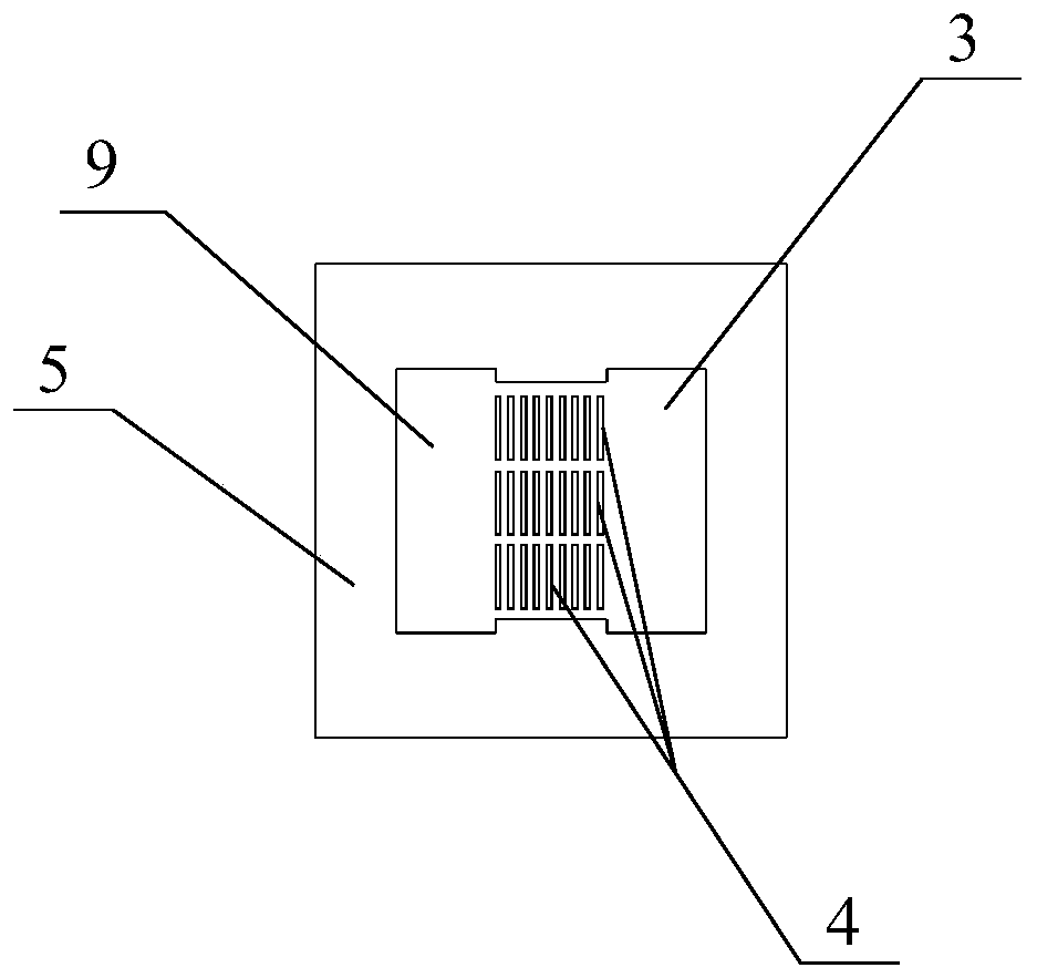
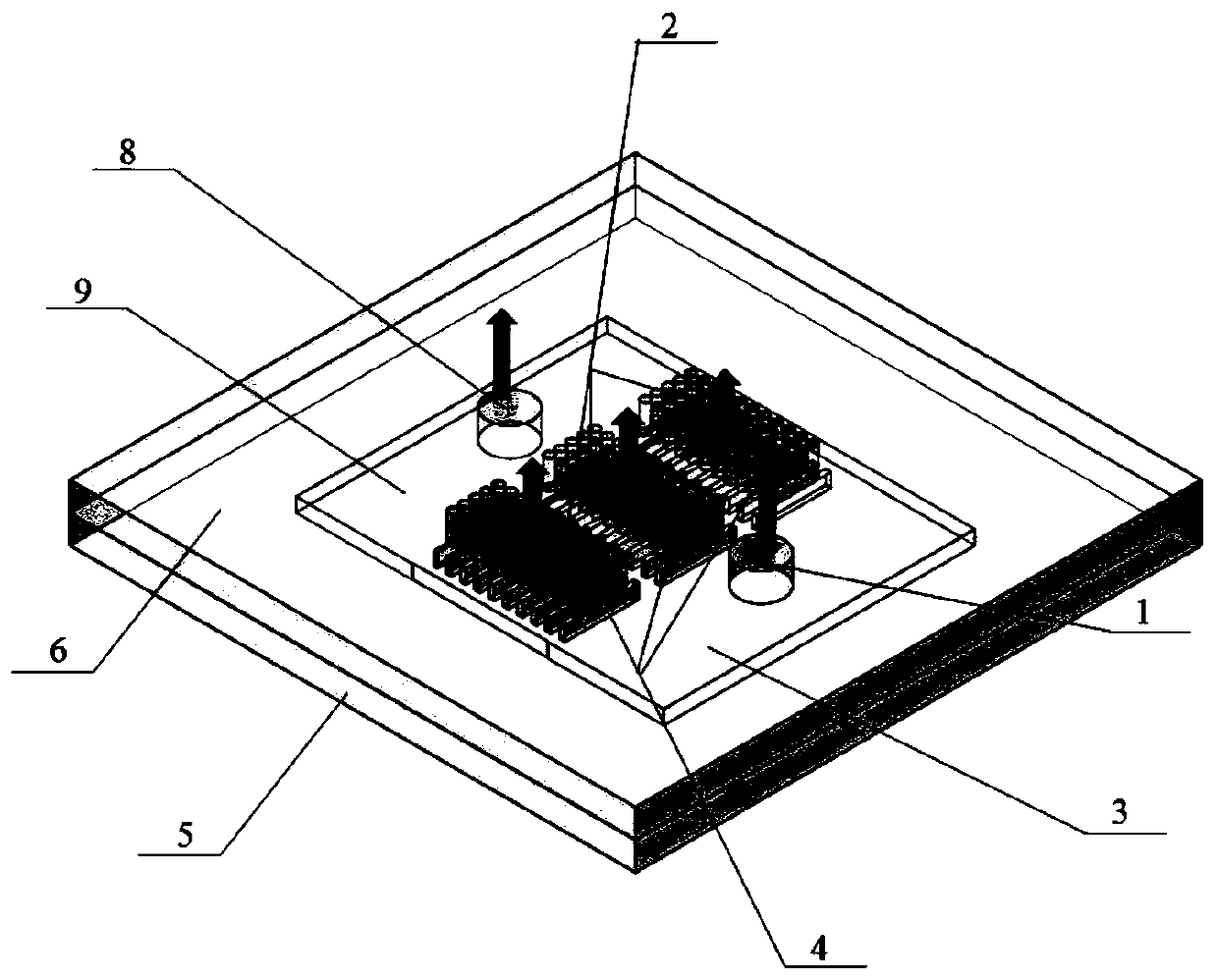
[0045] With the development of the performance of high-power electronic devices, GaN HEMT devices are widely used. Because the cost of electronic devices is too high, in the present invention, the heating film of the platinum-coated layer on the bottom surface of the lower substrate 6 is used to simulate the actual heating of electronic devices. ,like Figure 4 shown. In practical applications, the overall area and position of the microchannel and nanoporous region can be changed according to the size of the GaN HEMT device and the distribution characteristics of the hot zone. In this example, the specific structural size of the microchannel, and the pore size and interval size of the nanoporous Figure 6 shown. The wall thickness of the microchannel is 5um, the channel width is 20um, the upper and lower height of the channel is 20um, the diameter of the nanopore is 0.1um, the interval is 0.2um, and the upper and lower thickness is 0.4um.
[0046] The present invention uses ...
PUM
 Abstract
Description
Claims
Application Information
 - R&D
- Intellectual Property
- Life Sciences
- Materials
- Tech Scout
- Unparalleled Data Quality
- Higher Quality Content
- 60% Fewer Hallucinations
Browse by: Latest US Patents, China's latest patents, Technical Efficacy Thesaurus, Application Domain, Technology Topic, Popular Technical Reports.
© 2025 PatSnap. All rights reserved.Legal|Privacy policy|Modern Slavery Act Transparency Statement|Sitemap|About US| Contact US: help@patsnap.com


