System-level packaging process for radio frequency chip

A technology of system-level packaging and radio frequency chips, which is applied in the manufacture of electrical components, electrical solid devices, semiconductor/solid devices, etc., can solve the problems of increasing process difficulty and high-frequency signal interference, and achieve the effect of simplifying the process and protecting the integrity

Active Publication Date: 2019-07-12
浙江集迈科微电子有限公司
View PDF5 Cites 4 Cited by
  • Summary
  • Abstract
  • Description
  • Claims
  • Application Information

AI Technical Summary

Problems solved by technology

[0009] However, in practical applications, the adapter board at the bottom is not only used as a carrier board to paste chips and dissipate heat, but also as a signal lead-out structure and a connection structure to the PCB or substrate. Usually, the chip is directly pasted on the heat dissipation metal of the adapter board. Then lead the signal to the line of the adapter

Method used


Image

  • System-level packaging process for radio frequency chip
  • System-level packaging process for radio frequency chip
  • System-level packaging process for radio frequency chip

Examples


Embodiment approach 2

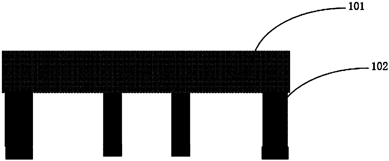
[0050] 201) making TSV, RDL, and metal bumps 103 on the base 101;

[0051] like Figure 4 As shown, TSV holes are formed on the surface of the base 101 by photolithography and etching processes. The diameter of the TSV holes ranges from 1um to 1000um, and the depth of the TSV holes ranges from 10um to 1000um; an insulating layer such as silicon oxide or silicon nitride is deposited on the base 101, or directly Thermal oxidation, the thickness of the insulating layer ranges from 10nm to 100um; a seed layer is made on the insulating layer by physical sputtering, magnetron sputtering or evaporation process, the thickness of the seed layer ranges from 1nm to 100um, which can be one layer or It can be multi-layer, and the metal material can be titanium, copper, aluminum, silver, palladium, gold, thallium, tin, nickel, etc.;

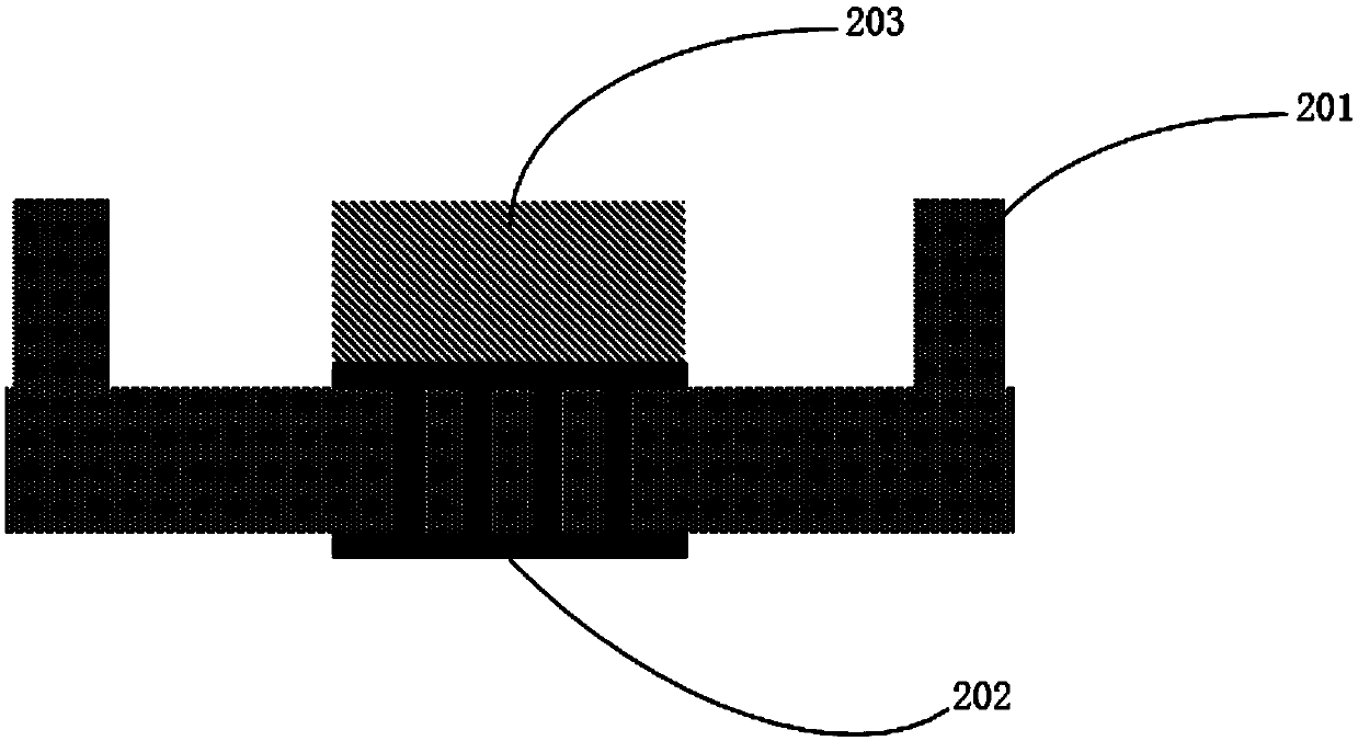
[0052] By electroplating copper, the copper metal is filled with the TSV hole 202 to form a copper column, which is densified at a temperature of 200 to 500 ...


PUM

PropertyMeasurementUnit
Diameteraaaaaaaaaa
Thicknessaaaaaaaaaa
Thicknessaaaaaaaaaa

Abstract

The invention discloses a system-level packaging process for a radio frequency chip. The process comprises the following steps of (101) base processing, (102) cover plate processing, and (103) packaging. The present invention provides the system-level packaging process for the radio frequency chip, different structures are separately made on different adapter boards, the process is simplified, andthe integrity of a high-frequency signal is protected.

Description

technical field [0001] The invention relates to the technical field of semiconductors, and more specifically, it relates to a system-in-package process of radio frequency chips. Background technique [0002] Microwave and millimeter wave radio frequency integrated circuit technology is the foundation of modern national defense weaponry and Internet industry. Millimeter-wave radio frequency integrated circuits also have huge actual needs and potential markets. [0003] In the context of the post-Moore's Law era, it has become more difficult to increase integration through the traditional way of reducing the size of transistors. The current electronic system is developing in the direction of miniaturization, diversification, and intelligence, and will eventually form a highly integrated and low-cost comprehensive electronic system that integrates multiple functions such as perception, communication, processing, and transmission. The core technology of the multifunctional int...

Claims


Application Information

Patent Timeline
IPC IPC(8): H01L21/50H01L21/60H01L23/367H01L23/552H01L23/48
CPCH01L21/50H01L23/367H01L23/481H01L23/552H01L24/81H01L2224/81805
Inventor 冯光建陈雪平刘长春丁祥祥王永河马飞程明芳郁发新
Owner 浙江集迈科微电子有限公司
Why Eureka
Try Eureka