Electromagnetic band gap (EBG) structure based printed circuit board and design method thereof

A technology of printed circuit boards and design methods, applied in the directions of printed circuits, printed circuits, printed circuit components, etc., can solve the problems of poor signal integrity of EBG structure, increase inductance value, etc., to achieve good bandwidth, increase the number of cells, capacitance, etc. The effect of value reduction

Inactive Publication Date: 2019-07-12
SUZHOU LANGCHAO INTELLIGENT TECH CO LTD
View PDF7 Cites 7 Cited by
  • Summary
  • Abstract
  • Description
  • Claims
  • Application Information

AI Technical Summary

Problems solved by technology

[0011] The purpose of the present invention is to provide a printed circuit board based on the electromagnetic energy gap EBG structure and its design method, aiming at solving the problem of poor signal integrity of the EBG structure in the prior art, realizing increasing the inductance value and improving the signal integrity of the EBG

Method used


Image

  • Electromagnetic band gap (EBG) structure based printed circuit board and design method thereof
  • Electromagnetic band gap (EBG) structure based printed circuit board and design method thereof
  • Electromagnetic band gap (EBG) structure based printed circuit board and design method thereof

Examples


Embodiment Construction

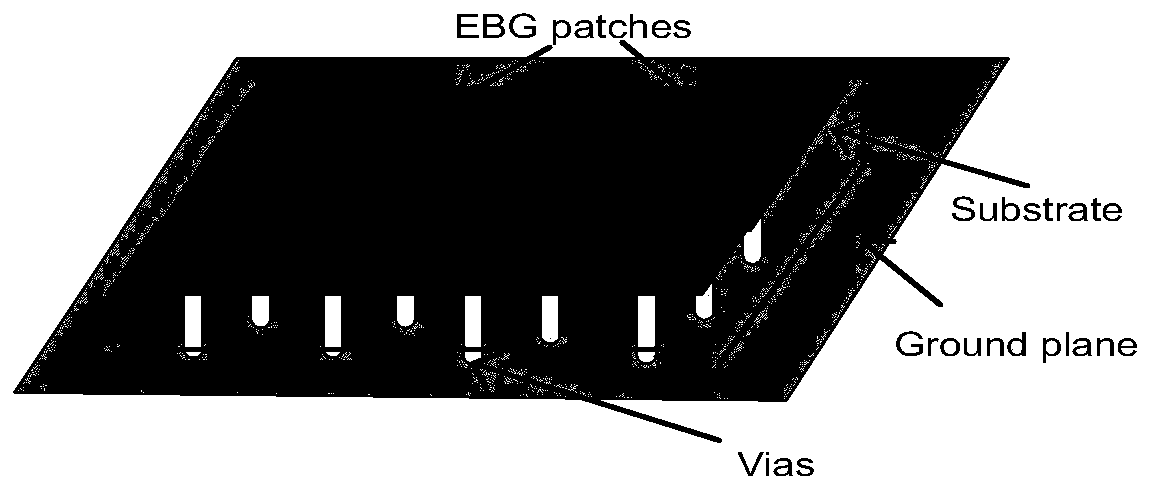
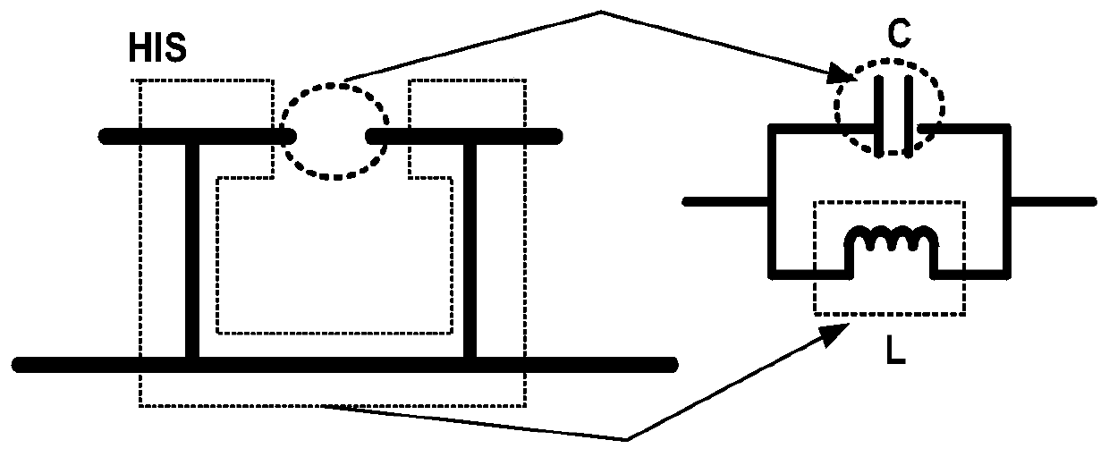
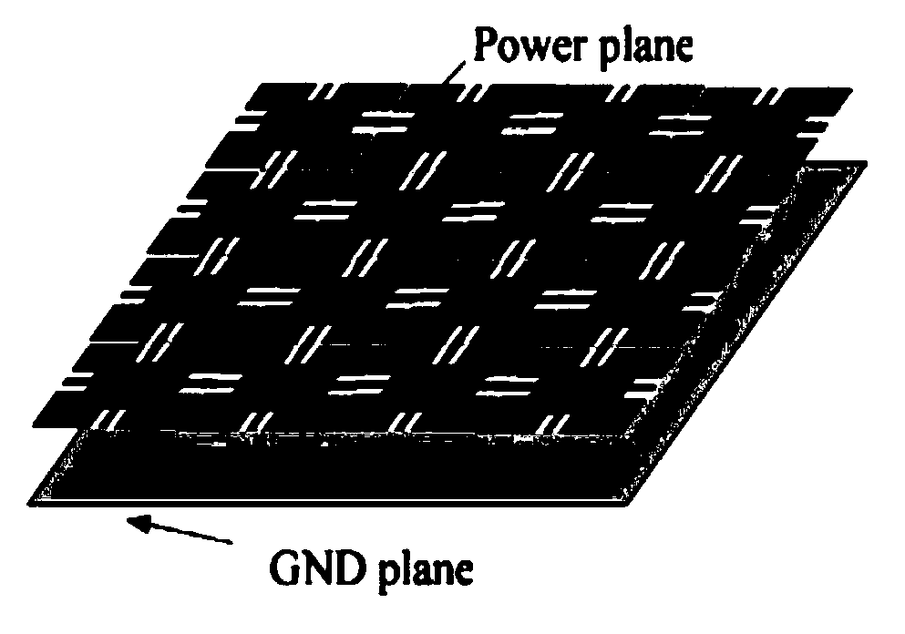
[0038] In order to clearly illustrate the technical features of the present solution, the present invention will be described in detail below through specific implementation methods and in conjunction with the accompanying drawings. The following disclosure provides many different embodiments or examples for implementing different structures of the present invention. To simplify the disclosure of the present invention, components and arrangements of specific examples are described below. Furthermore, the present invention may repeat reference numerals and / or letters in different instances. This repetition is for the purpose of simplicity and clarity and does not in itself indicate a relationship between the various embodiments and / or arrangements discussed. It should be noted that components illustrated in the figures are not necessarily drawn to scale. Descriptions of well-known components and processing techniques and processes are omitted herein to avoid unnecessarily lim...


PUM


Abstract

The invention provides an electromagnetic band gap structure based printed circuit board and a design method thereof. A metal coil is added to an original linear channel, the metal wire is bent so that the linear channel is turned into channel with multiple folds, the channel is cut, the unit number is increased, and EBG design is realized. According to simulation, the channel coiling length is increased so that an inductance value is added and the capacitance is reduced, the bandwidth can be increased, and the cutoff depth and central frequency can move towards the high frequency. Compared with an EBG with the traditional linear channel, the multi-fold channel EBG is higher in the noise inhibition bandwidth and cutoff depth, the signal quality is higher in the aspect of integrity, the EBGcan be applied to a multi-layer PCB, channel cutting can be made in the power layer, the unit number is increased, and an extra power layer is not needed.

Description

technical field [0001] The invention relates to the technical field of digital circuits, in particular to a printed circuit board based on an electromagnetic energy gap EBG structure and a design method thereof. Background technique [0002] In recent years, due to the trend of faster and faster speed in high-frequency digital circuits, the signal will be interfered by many factors during the transmission process. At this time, the integrity of the signal is particularly important. When the signal is transmitted from the transmitting end to the receiving end Sometimes the waveform may be interfered and damaged to cause the received signal to be distorted. Image factors may include signal pair timing problems, signal ringing, signal reflection, near-end and long-range crosstalk, switching noise, ground bounce and power bounce, Attenuation, capacitive load, electromagnetic radiation, battery interference, etc., so reducing noise is the best way to maintain the signal. [0003...

Claims


Application Information

Patent Timeline
Patent Type & Authority Applications(China)
IPC IPC(8): H05K1/02
CPCH05K1/0236H05K1/025H05K2201/0776
Inventor 王敬文
Owner SUZHOU LANGCHAO INTELLIGENT TECH CO LTD
Why Eureka
Try Eureka