

Semiconductor structure and forming method thereof
A semiconductor and annular groove technology, applied in the fields of semiconductor devices, semiconductor/solid-state device manufacturing, semiconductor/solid-state device components, etc., can solve the problem of the sealing performance of the chip sealing ring needs to be improved, to prevent corrosion, avoid stress damage, improve The effect of protection
- Summary
- Abstract
- Description
- Claims
- Application Information
AI Technical Summary
Problems solved by technology
Method used
Image

Examples
no. 1 example
[0031] Figure 1 to Figure 7 This is a schematic diagram of the structure corresponding to each step of the semiconductor structure forming method in this embodiment.
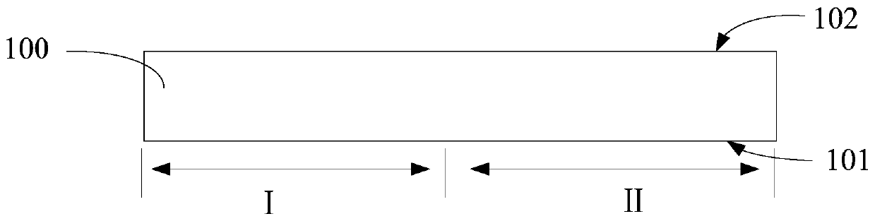
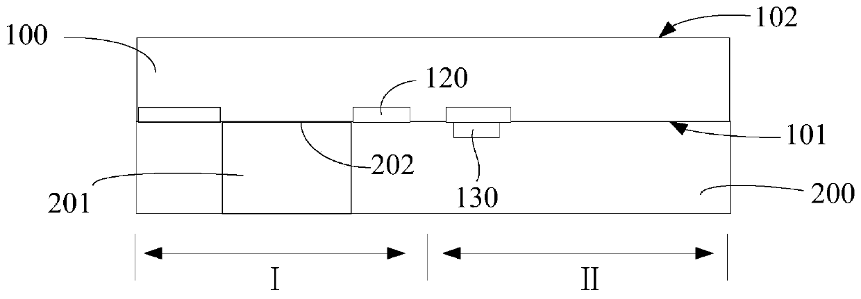
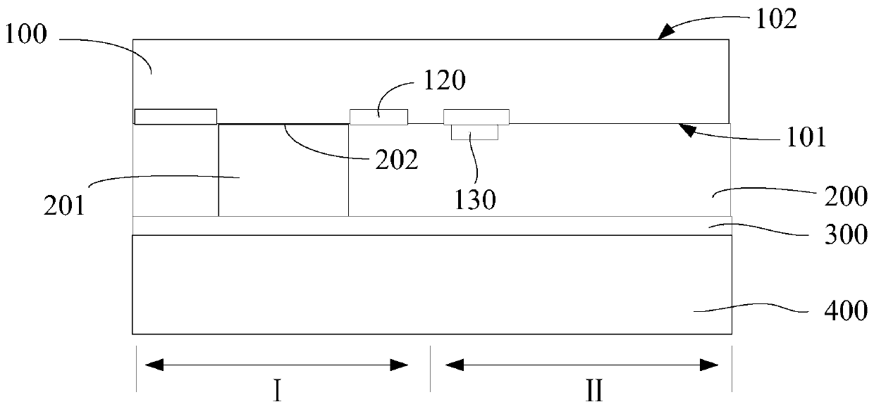
[0032] reference figure 1 , A semiconductor substrate 100 is provided. The semiconductor substrate 100 includes a device region II and a sealing region I surrounding the device region II. The semiconductor substrate 100 has a first surface 101 and a first surface 101 opposite to the first surface 101. The second surface 102.
[0033] The material of the semiconductor substrate 100 is silicon, germanium, silicon germanium, silicon carbide, gallium arsenide or indium gallium, and the substrate 100 can also be a silicon-on-insulator substrate or a germanium-on-insulator substrate. In this embodiment, the substrate 100 is a silicon substrate.
[0034] reference figure 2 , The front side process is performed on the semiconductor substrate 100, that is, a number of isolation trench (STI) components 120 are formed in the s...
no. 2 example
[0061] The difference between this embodiment and the first embodiment is only the difference in the annular groove, so the steps before forming the annular groove are as in the first embodiment Figure 1 to 4 , I won’t repeat it here. Figure 8 to Figure 12 This embodiment provides a schematic diagram of some steps of the method for forming a semiconductor structure.
[0062] reference Figure 8 , A patterned layer 600 is formed on the surface of the dielectric layer 500.
[0063] Specifically, the patterned layer 600 of the sealing area I has a first opening 601, and the patterned layer 600 of the device area II has a second opening 602.
[0064] In this embodiment, the material of the patterned layer 600 is silicon nitride.
[0065] In other embodiments, the material of the patterned layer 600 may also be silicon oxide.
[0066] reference Picture 9 , Using the patterned layer 600 as a mask to etch the dielectric layer 500 and the semiconductor substrate 100 to form a groove penetra...
PUM
 Abstract
Description
Claims
Application Information