Ferroelectric/piezoelectric field effect transistor and preparation method thereof

A piezoelectric field and effect tube technology, which is used in semiconductor/solid-state device manufacturing, circuits, electrical components, etc. to reduce operating power consumption, reduce sub-threshold swing, and improve on/off speed.

Inactive Publication Date: 2019-07-19
SHANGHAI HUALI INTEGRATED CIRCUTE MFG CO LTD
View PDF5 Cites 4 Cited by
  • Summary
  • Abstract
  • Description
  • Claims
  • Application Information

AI Technical Summary

Problems solved by technology

However, none of these methods can make the sub-thresh

Method used


Image

  • Ferroelectric/piezoelectric field effect transistor and preparation method thereof
  • Ferroelectric/piezoelectric field effect transistor and preparation method thereof
  • Ferroelectric/piezoelectric field effect transistor and preparation method thereof

Examples


preparation example Construction

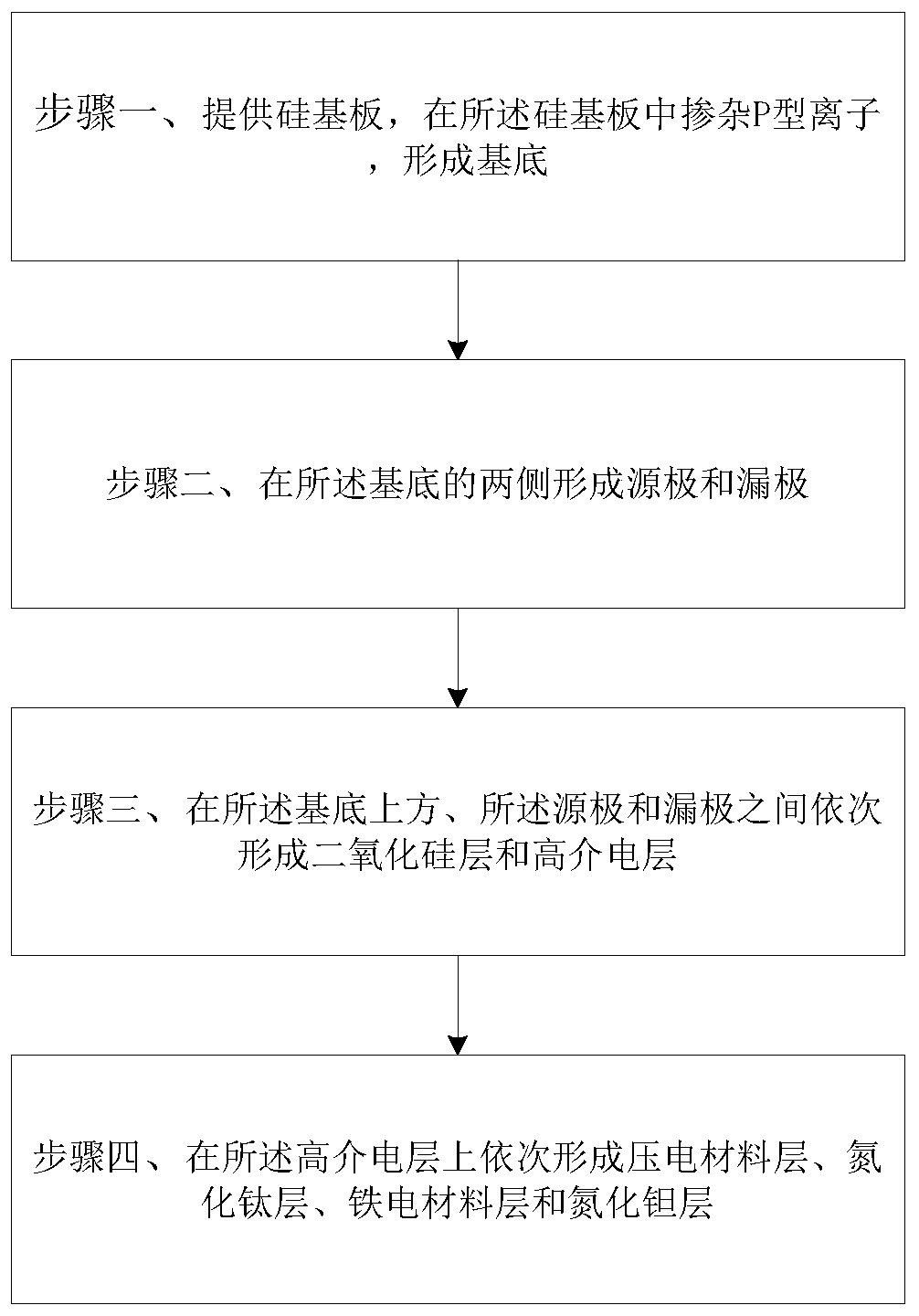
[0034] The present invention also includes the preparation method of the iron / piezoelectric field effect tube, refer to figure 2 , figure 2 Shown is the flow chart of the preparation method of the iron / piezoelectric field effect tube of the present invention. The method at least includes the following steps:

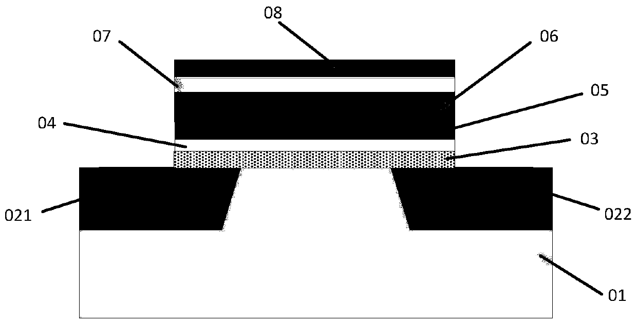
[0035] Step 1, providing a silicon substrate, doping P-type ions in the silicon substrate to form the base 01; that is to say, the formation of the P-type base is by implanting P-type ions into the silicon material plate, so as to form figure 1 The P-type substrate 01 shown is thus the NMOS field effect transistor of this embodiment.

[0036] Step 2, forming a source 021 and a drain 022 on both sides of the substrate 01, and the source 021 and the drain 022 serve as the source and drain of an NMOS field effect transistor;

[0037] Step 3: Form a silicon dioxide layer 03 and a high dielectric layer 04 sequentially above the substrate 01 and between the source 021 and...


PUM


Abstract

The invention provides a ferroelectric /piezoelectric field effect transistor and a preparation method thereof. The iron/piezoelectric field effect transistor comprises a substrate, a source electrode, a drain electrode and a gate electrode. The gate electrode comprises silicon dioxide, a high dielectric layer, a piezoelectric material layer, a titanium nitride layer, a ferroelectric material layer and a tantalum nitride layer, which are sequentially stacked from bottom to top. The preparation method comprises the following steps: providing a silicon substrate, and doping P-type ions into thesilicon substrate to form a substrate; forming a source electrode and a drain electrode at two sides of the substrate; sequentially forming the silicon dioxide layer and the high dielectric layer between the source electrode and the drain electrode above the substrate; and sequentially forming the piezoelectric material layer, the titanium nitride layer, the ferroelectric material layer and the tantalum nitride layer on the high dielectric layer. Based on the field effect transistor, the ferroelectric material and the piezoelectric material are introduced into the gate electrode, and the negative capacitance effect of the ferroelectric material and the electrostrictive effect of the piezoelectric material are used for jointly achieving the voltage amplification function. The working voltage of the device is reduced, the subthreshold swing is reduced, the on/off speed of the device is improved, and the working power consumption is further reduced.

Description

technical field [0001] The invention relates to the field of design and manufacture of semiconductor devices, in particular to an iron / piezoelectric field effect transistor and a preparation method thereof. Background technique [0002] With the improvement of the integration density of CMOS devices, the increasing power consumption will become an important bottleneck restricting the further development of integrated circuits. Reducing the operating voltage by reducing the sub-threshold swing of the device is an effective means to reduce the power consumption. The field effect transistor with negative capacitance effect is an effective technical solution to realize this purpose. [0003] At present, the sub-threshold swing value is reduced by adjusting the gate oxide layer structure and thickness composition, channel structure and material, thereby reducing device power consumption. However, none of these methods can make the subthreshold swing smaller than 60mV / decade (an...

Claims


Application Information

Patent Timeline
IPC IPC(8): H01L29/423H01L29/43H01L21/336H01L29/78
CPCH01L29/42312H01L29/43H01L29/66477H01L29/78
Inventor 陕皓
Owner SHANGHAI HUALI INTEGRATED CIRCUTE MFG CO LTD
Why Eureka
Try Eureka