Low-cost TMBS device structure and manufacturing method

A manufacturing method and device structure technology, applied in the direction of semiconductor/solid-state device manufacturing, semiconductor devices, electrical components, etc., can solve the problems of silicon surface damage, poor reliability of use, complicated process steps, etc., and achieve reduced corrosion thickness and weakening. The effect of electric field concentration and area increase

Inactive Publication Date: 2019-07-23
江苏新顺微电子股份有限公司
View PDF7 Cites 11 Cited by
  • Summary
  • Abstract
  • Description
  • Claims
  • Application Information

AI Technical Summary

Problems solved by technology

However, with the dry etching process, it is inevitable that there will be damage to the silicon surface, and the Schottky contact is a process that is very sensitive to the state of the silicon surface. The etched silicon damage will cause the instability of the Schottky contact. Reliability becomes poor; therefore, in order to solve this problem, the traditional TMBS structure adopts a high-temperature furnace tube thermal oxidation process to grow a thin layer of sacrificial oxide layer after dry etching, and then removes it by wet etching process to achieve Repair etch damage on silicon surfaces
The whole process steps are more cumbersome
[0021] 3. In the traditional TMBS device structure, although the sacrificial oxide layer process is used to repair the damage caused by the dry etching process, in the actual tape-out verification, it is found that the damaged layer has not been completely repaired, and PVD deposition in step 11 is still required. After the Tertky barrier metal layer, the Schottky contact is formed through a relatively high alloy temperature, and then the electrode metal is deposited; and if the Schottky barrier metal and the electrode metal are deposited continuously at one time, due to the commonly used deposition Deposited metals are not resistant to high temperatures, and the alloy temperature is too high, the Schottky barrier metal and the electrode metal will alloy with each other, thus affecting the Schottky contact

Method used


Image

  • Low-cost TMBS device structure and manufacturing method
  • Low-cost TMBS device structure and manufacturing method

Examples


Embodiment Construction

[0045] The present invention will be further described in detail below in conjunction with the accompanying drawings and embodiments.

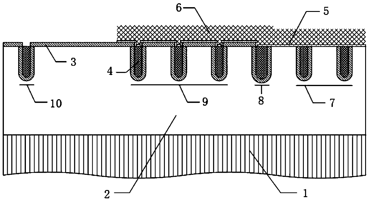
[0046] like figure 1 Shown, a kind of low-cost TMBS device structure among the present embodiment, it comprises as substrate densely doped silicon substrate 1; On densely doped silicon substrate 1, be provided with lightly doped silicon epitaxial layer 2; A silicon groove array is arranged on the silicon epitaxial layer 2, and the silicon groove array includes a cut-off groove 10, an extension groove 9, a large original cell groove 8, and several original cell grooves 7 arranged at horizontal intervals; each groove has Unused functions. A SiO2 layer 3 with a certain thickness is formed on the inner sidewall of the silicon trench array and the surface of the lightly doped silicon epitaxial layer 2; the interior of the silicon trench array is filled with heavily doped Poly4, and the top surface of the heavily doped Poly4 and the lightly doped s...


PUM


Abstract

The invention relates to a low-cost TMBS device structure and a manufacturing method, and belongs to the technical field of integrated circuit or discrete device manufacturing. The low-cost TMBS device structure comprises a heavily doped silicon substrate, wherein a lightly doped silicon epitaxial layer is arranged on the heavily doped silicon substrate; a silicon groove array is arranged on the lightly doped silicon epitaxial layer; a SiO2 layer is arranged on the inner side wall of the silicon groove array; the silicon groove array is filled with a heavily doped Poly; a Schottky barrier metal layer is arranged on the silicon groove array; and an electrode metal layer is arranged on the Schottky barrier metal layer. The silicon groove array comprises a primitive cell trench unit, a primitive cell large trench, an extension trench and a cut-off trench, Schottky barrier metal layers are arranged on the upper surfaces of the primitive cell trench unit and the primitive cell large trench,and a SiO2 layer and a Schottky barrier metal layer are arranged on the lightly doped silicon epitaxial layer between the primitive cell large trench and the extension trench. According to the invention, the process steps are reduced, the terminal structure is optimized, the terminal electric field distribution is more uniform, and the breakdown voltage is improved; and the forward voltage drop of the device is reduced.

Description

technical field [0001] The invention relates to a low-cost TMBS device structure and a manufacturing method, belonging to the technical field of integrated circuit or discrete device manufacturing. Background technique [0002] TMBS is the abbreviation of Trench MOS Barrier Schottky Diode in English. It is a new type of low-power Schottky diode rectifier device, which has a lower forward voltage drop than ordinary planar Schottky diodes; but correspondingly, the TMBS device The process steps are cumbersome, and the process requirements and manufacturing costs are also higher than those of planar Schottky diodes. [0003] The traditional TMBS device structure includes a heavily doped silicon substrate as a substrate; a lightly doped silicon epitaxial layer is provided on the heavily doped silicon substrate; an array of silicon trenches with different functions is provided on the silicon epitaxial layer, including stop trenches Groove, primary cell large groove, primary cell ...

Claims


Application Information

Patent Timeline
Patent Type & Authority Applications(China)
IPC IPC(8): H01L29/872H01L21/329
CPCH01L29/8725H01L29/66143
Inventor 陈晓伦韩笑陈烨徐永斌
Owner 江苏新顺微电子股份有限公司
Why Eureka
Try Eureka