
A method of manufacturing a grain boundary layer capacitor

A manufacturing method and capacitor technology, applied in the direction of capacitors, fixed capacitors, components of fixed capacitors, etc., can solve the problems of difficult to accurately control technology, large differences in capacitors, affecting stability, etc., to achieve good consistency and improved resistance value. , The effect of improving the consistency of resistance

Inactive Publication Date: 2021-07-02
TAIYUAN UNIVERSITY OF SCIENCE AND TECHNOLOGY +2
View PDF5 Cites 0 Cited by
  • Summary
  • Abstract
  • Description
  • Claims
  • Application Information

AI Technical Summary

Problems solved by technology

Theoretically, the thicker the space charge layer at the grain boundary, the greater the resistance value of the grain boundary layer capacitor, but at the same time, due to the increase in the thickness of the space charge region, the capacitance of the capacitor will decrease rapidly, so in practice, the capacitance of the capacitor is often sacrificed value to obtain high resistance and voltage increase, but doing so may outweigh the gain in practical applications
On the other hand, acceptor ions and glass substances (insulating substances) in the grain boundary layer enter the grain boundary through thermal diffusion, but this process is extremely difficult to control precisely in technology, so in actual products, the resistance value of the capacitor is often different. Large, poor consistency, affecting the stability of product use

Method used


Image

  • A method of manufacturing a grain boundary layer capacitor
  • A method of manufacturing a grain boundary layer capacitor
  • A method of manufacturing a grain boundary layer capacitor

Examples


Embodiment Construction

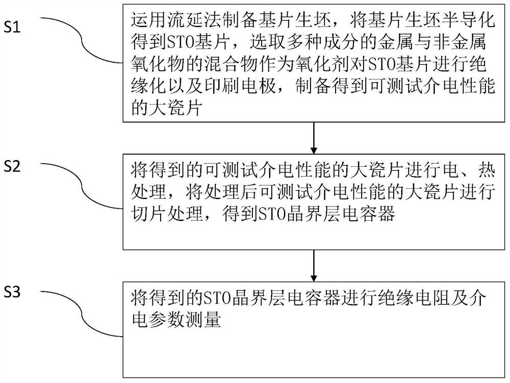
[0032] The present invention will be described in further detail below in conjunction with accompanying drawing, the present invention provides a kind of manufacturing method of grain boundary layer capacitor, as figure 1 As shown, the method includes the following steps:

[0033] S1. Use the tape casting method to prepare the substrate green body, semiconduct the substrate green body to obtain the STO substrate, select a mixture of metal and non-metal oxides with various components as the oxidant to insulate the STO substrate and print electrodes , to prepare a large ceramic piece that can be tested for dielectric properties;

[0034] Wherein, the step S1 includes the following steps:

[0035] S11, using tape casting method to prepare green body, wherein, using SrCO 3 and TiO 2 As the main ingredient, defoamer and dispersant are added, and 1% of the weight of the main ingredient is taken each, and the casting slurry is obtained by ball milling in a planetary ball mill, and t...


PUM

PropertyMeasurementUnit
sizeaaaaaaaaaa
electrical resistanceaaaaaaaaaa

Abstract

The invention provides a method for manufacturing a grain boundary layer capacitor, which adopts a three-step method to prepare the STO grain boundary layer capacitor. First, the STO green ceramic sheet is sintered in a reducing atmosphere to obtain a semiconducting substrate, and then an appropriate oxidant is selected to insulate the STO semiconducting substrate, and finally the resistance value of the STO grain boundary layer capacitor increases with the load voltage and pressurization time. Under the condition of loading voltage, rapid heat treatment is performed on the capacitance of the grain boundary layer to improve the insulation resistance value and consistency of the capacitor. The effect of this method is obvious, for SrTiO 3 The application of grain boundary layer capacitors in microwave integration technology, microwave circuits and microwave communications is of great significance.

Description

technical field [0001] The invention relates to the technical field of semiconductors and electronic functional materials, and particularly designs a method for manufacturing a grain boundary layer capacitor. Background technique [0002] Grain boundary layer capacitors have the advantages of small size, large dielectric constant, wide application temperature range (-55℃~125℃), high capacitance temperature stability (≤±4.0%~≤±25%) and good frequency stability characteristics. It is widely used in microwave circuits and microwave communications. Single-layer chip grain boundary layer capacitors generally use SrTiO 3 (STO) or electron-doped STO is used as the parent phase, which is made by one-step or two-step method. The one-step method is that the semiconducting and insulating of STO are completed in the same sintering. The two-step method is to first sinter STO in a reducing N2 / H2 mixed atmosphere at a high temperature above 1300 ° C to form a semiconductive ceramic shee...

Claims


Application Information

Patent Timeline
Patent Type & Authority Patents(China)
IPC IPC(8): H01G4/12H01G4/00
CPCH01G4/00H01G4/1281
Inventor 杨昌平李伟恒胡竞楚张木森徐玲芳梁世恒王瑞龙肖海波
Owner TAIYUAN UNIVERSITY OF SCIENCE AND TECHNOLOGY
Learn More