Preparation method of large-area perovskite solar cell
A solar cell and perovskite technology, applied in the field of solar photovoltaic, can solve the problems of excess PbI residue, high film roughness, easy formation of holes, etc., and achieves the effect of simple and feasible preparation method, uniform and flat film layer, and reduced residue.
- Summary
- Abstract
- Description
- Claims
- Application Information
AI Technical Summary
Problems solved by technology
Method used
Image
Examples
preparation example Construction
[0027] The preparation steps of the perovskite absorbing layer are: spraying PbI on the electron transport layer or the hole transport layer 2 solution to obtain a lead iodide thin film layer; scraping the mixed solution of FAI / MACl / MABr on the lead iodide thin film layer to obtain a perovskite absorption layer.
[0028] Among them, the perovskite absorbing layer is first sprayed with lead iodide (PbI 2 ) solution, annealed to form PbI 2 thin film layer; then in PbI 2 A mixed solution of FAI / MACl / MABr (formamidine ion (FA) and methylammonium ion (MA)) is scraped on the film layer and annealed to obtain a perovskite layer. Preparation of PbI by spraying method 2 The thin film layer can make it have higher roughness, and when scraping the FAI / MACl / MABr mixed solution, it can ensure that the solution is fully immersed, making the reaction more complete and reducing PbI 2 residues, thereby reducing the adverse effect on the perovskite layer; the film layer prepared by this met...
Embodiment 1
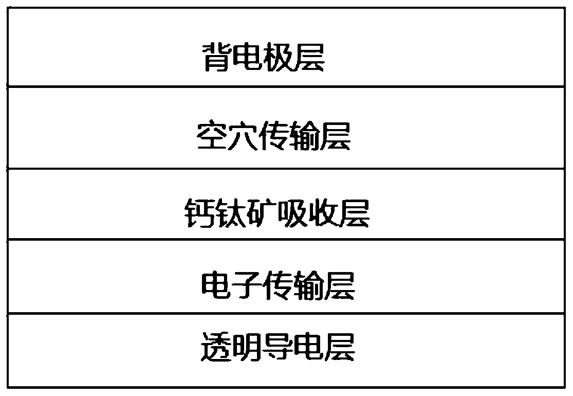
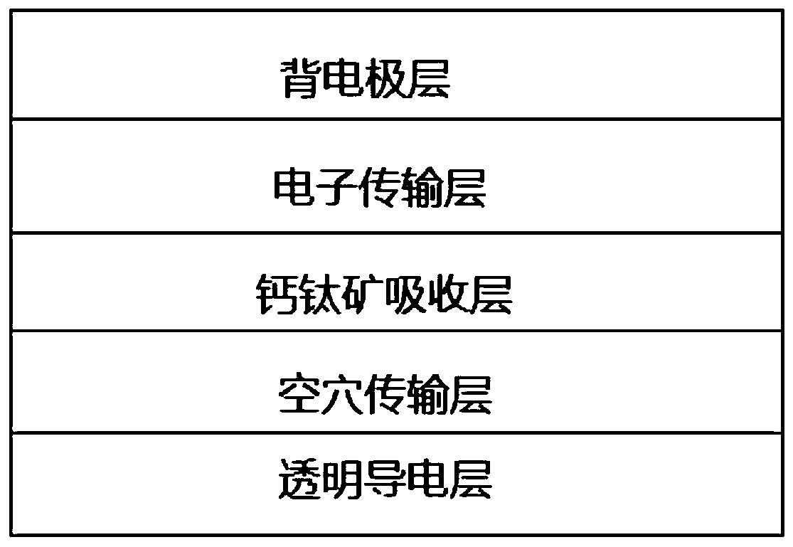
[0040] like figure 1 In the formal structure of the perovskite solar cell shown, a transparent conductive layer, an electron transport layer, a perovskite absorbing layer, a hole transport layer and a back electrode layer are sequentially arranged, and the specific preparation method is as follows:
[0041] 1) Scrape-coat SnO on the 25cm×25cm ITO transparent conductive layer 2 , annealed at 150°C to obtain an electron transport layer with a thickness of 20nm;
[0042] 2) The perovskite absorbing layer was prepared by scraping and spraying on the electron transport layer: the spraying concentration on the electron transport layer was 1.15mol / LPbI 2 DMF solution, annealed at 150°C to obtain PbI with a thickness of 150nm 2 Thin film layer; in PbI 2 Add the FAI / MACl / MABr mixed solution dropwise on the film layer, scrape the mixed solution, and anneal at 150°C to obtain a perovskite layer with a thickness of 300nm;
[0043] 3) Scrape-coat Spiro-OMeTAD on the prepared perovskite...
Embodiment 2
[0046] like figure 1 In the formal structure of the perovskite solar cell shown, a transparent conductive layer, an electron transport layer, a perovskite absorbing layer, a hole transport layer and a back electrode layer are sequentially arranged, and the specific preparation method is as follows:
[0047] 1) Scrape-coat SnO on the 25cm×25cm ITO transparent conductive layer 2 , annealed at 150°C to obtain an electron transport layer with a thickness of 30nm;
[0048] 2) The perovskite absorbing layer was prepared by scraping and spraying on the electron transport layer: the spraying concentration on the electron transport layer was 1.3mol / LPbI 2 DMF solution, annealed at 150°C to obtain PbI with a thickness of 200nm 2 Thin film layer; in PbI 2 Add the FAI / MACl / MABr mixed solution dropwise on the film layer, scrape the mixed solution, and anneal at 150°C to obtain a perovskite layer with a thickness of 350nm;
[0049] 3) Scrape-coat Spiro-OMeTAD on the prepared perovskite ...
PUM
| Property | Measurement | Unit |
|---|---|---|
| Concentration | aaaaa | aaaaa |
| Thickness | aaaaa | aaaaa |
| Thickness | aaaaa | aaaaa |
Abstract
Description
Claims
Application Information

