A kind of preparation method of ultra-thin crystalline silicon double-sided solar cell

A solar cell and crystalline silicon technology, applied in the field of solar cells, can solve the problems of poor product diffusion junction uniformity, high breakage rate of thin silicon wafers, and difficulty in realizing industrialization, so as to increase the duration of light stay and improve the utilization rate of light energy. , the effect of reducing the breakage rate

Active Publication Date: 2020-12-18
HEBEI UNIVERSITY
View PDF6 Cites 0 Cited by
  • Summary
  • Abstract
  • Description
  • Claims
  • Application Information

AI Technical Summary

Problems solved by technology

[0005] The purpose of the present invention is to provide a method for preparing ultra-thin crystalline silicon double-sided solar cells with simple process, which can effectively reduce the product damage rate and improve product quality, so as to solve the problem of high damage rate, high cost and technical problems of existing thin silicon wafers. Complexity, poor uniformity of product diffusion junction and difficulty in industrialization

Method used


Image

  • A kind of preparation method of ultra-thin crystalline silicon double-sided solar cell
  • A kind of preparation method of ultra-thin crystalline silicon double-sided solar cell
  • A kind of preparation method of ultra-thin crystalline silicon double-sided solar cell

Examples


Embodiment 1

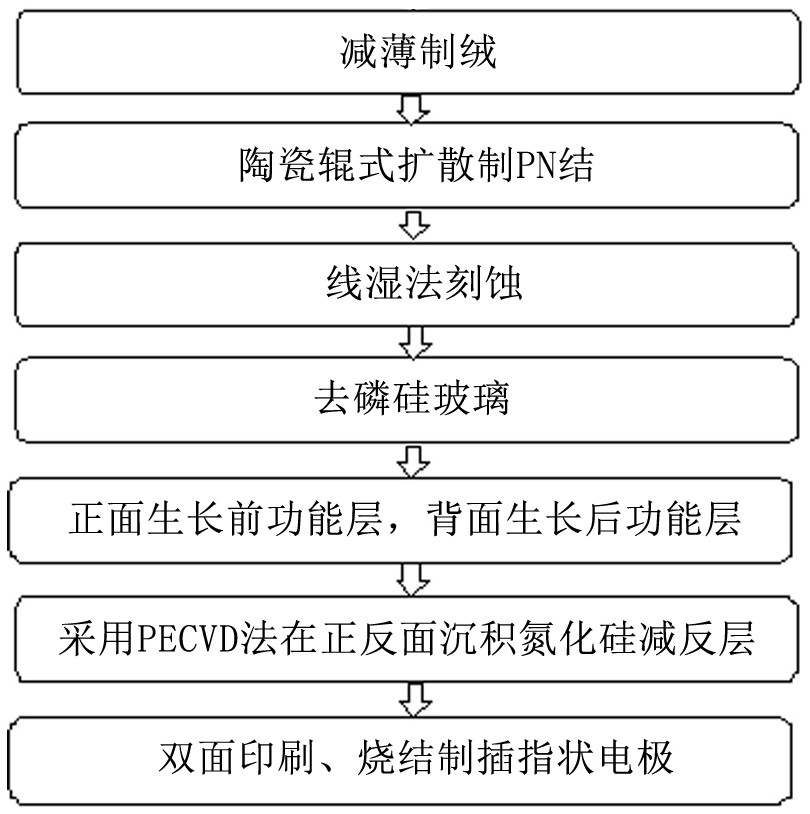
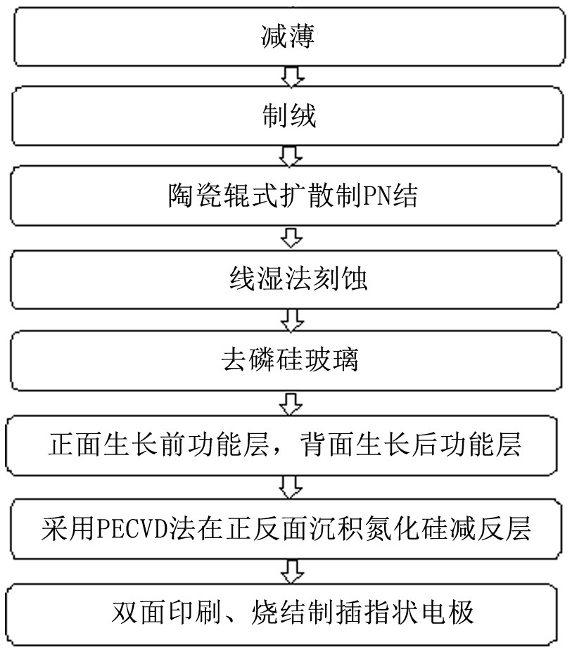
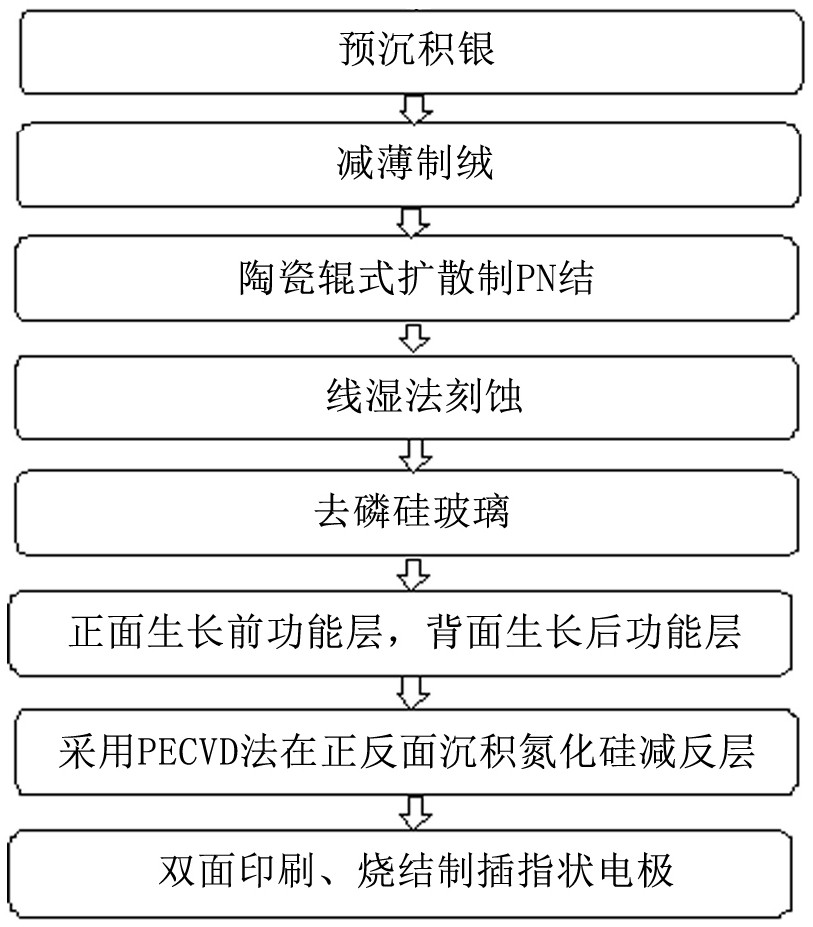
[0036] Such as figure 1 As shown, the preparation method of the ultra-thin crystalline silicon double-sided solar cell provided in this embodiment is as follows: Thinning texturing—ceramic roll diffusion to make PN junction—wire wet etching—phosphorous silicon glass removal—growth functional layer— Double-sided deposition of silicon nitride anti-reflection layer - screen printing, sintering finger electrode.

[0037] figure 1 Only the key steps in the present invention are shown, and some conventional processes such as cleaning are not listed here. The cleaning process includes cleaning before and after texturing. Before texturing, acetone and alcohol are generally used for ultrasonic cleaning to remove organic and inorganic impurities on the surface of the polysilicon substrate, and then cleaned with deionized water; after texturing, it is usually cleaned with Rinse with deionized water and blow dry with nitrogen. These conventional processes will not be described too much...

Embodiment 2

[0046] Thinning and texturing: place a 200μm thick P-type polysilicon substrate in HF, H 2 o 2 , silver nitrate and copper nitrate mixed solution, the mass fraction of HF is 35%, H 2 o 2 The mass fraction is 35%, the molar concentrations of silver nitrate and copper nitrate are 0.5mol / L and 0.3mol / L respectively, HF, H 2 o 2 The volume ratio of the additives (the additives here are silver nitrate and copper nitrate) is 3:2.5:1. Make the polysilicon substrate in HF, H 2 o 2 , silver nitrate and copper nitrate mixed solution at 25°C for 2200s, the polysilicon substrate is thinned to 100 μm, and the surface of the polysilicon substrate is made into a suede structure.

[0047] PN junction made by ceramic roller diffusion: prepare 4% phosphoric acid solution, and conduct ultrasonic atomization deposition on the thinned polysilicon substrate at 20°C (ultrasonic frequency is 1.8MHz, atomization rate is 2mL / min, and the median Diameter 4.0μm); then place the polysilicon substra...

Embodiment 3

[0054] Thinning and texturing: place a 220μm thick P-type polysilicon substrate in HF, H 2 o 2 and palladium nitrate mixed solution, the mass fraction of HF is 30%, H 2 o 2 The mass fraction is 38%, the molar concentration of palladium nitrate is 1.2mol / L, HF, H 2 o 2 The volume ratio of palladium nitrate and palladium nitrate is 4.5:2:1. Make the polysilicon substrate in HF, H 2 o 2 and palladium nitrate mixed solution at 23°C for 2000s, the thickness of the polysilicon substrate is reduced to 110 μm, and the surface of the polysilicon substrate is made into a textured structure.

[0055]PN junction made by ceramic roller diffusion: prepare 6% phosphoric acid solution, and conduct ultrasonic atomization deposition on the thinned polysilicon substrate at 22°C (ultrasonic frequency is 1.75MHz, atomization rate is 3mL / min, and the median Diameter 3.8μm); then place the polysilicon substrate on the ceramic roller, heat it to the temperature to be diffused by an infrared la...


PUM

PropertyMeasurementUnit
thicknessaaaaaaaaaa
thicknessaaaaaaaaaa
thicknessaaaaaaaaaa

Abstract

The invention provides a method for preparing ultrathin crystalline silicon double-sided solar cell. The method comprises steps of: firstly thinning a polycrystalline silicon substrate to 90-120[mu]mat 18-25 degrees centigrade for 2000-2300s by using a mixed solution of HF, H2O2 and an additive, wherein a textured structure is formed on the surface of the substrate during the thinning process; preparing a PN junction by roll diffusion, and using ultrasonic atomization of phosphoric acid, thereby being nontoxic and nonpolluting, and achieving a uniform diffusion junction; and disposing siliconnitride antireflection layers on the front and back sides of the substrate; finally forming finger electrodes on the front and back sides by a silk-screen printing and sintering process. The method is suitable for the production technology of polycrystalline silicon 90-120[mu]m thick. Compared with a method for preparing a conventional polycrystalline silicon cell 180[mu]m thick, the method can reduce the thickness of the cell under the premise of ensuring a fragmentation rate, ensures battery efficiency, is simple in process, and low in cost. The method also solves the problem that the thincell is likely to be bent and is fragile, and can be industrialized by experimental verification.

Description

technical field [0001] The invention relates to the field of solar cells, in particular to a preparation method of ultra-thin flexible crystalline silicon double-sided solar cells. Background technique [0002] Solar cells are one of the cleanest energy sources today, inexhaustible and inexhaustible. A solar cell is a device that converts light energy into electrical energy by using the photovoltaic effect of semiconductor materials. At present, crystalline silicon cells are still the mainstay in the market, and monocrystalline silicon and polycrystalline silicon are mainly used as photoelectric conversion materials. [0003] At present, the thickness of conventional crystalline silicon cells is generally 180μm-220μm. The problem with this type of crystalline silicon solar cells is that they are highly brittle and easily broken when bent. Generally speaking, when the thickness of the crystalline silicon cell decreases from 200 μm to below 120 μm, it can exhibit good flexi...

Claims


Application Information

Patent Timeline
Patent Type & Authority Patents(China)
IPC IPC(8): H01L31/18H01L31/068H01L31/0236H01L31/0216H01L31/0224
CPCY02E10/546Y02P70/50
Inventor 何仁陈静伟陈剑辉黄志平宋登元许颖
Owner HEBEI UNIVERSITY
Why Eureka
Try Eureka