A Controllable Thinning Method of Two-Dimensional Atomic Crystals of Transition Metal Chalcogenides
A technology of two-dimensional atomic crystals and transition metal chalcogenides, applied in chemical instruments and methods, crystal growth, single crystal growth, etc., can solve problems such as high energy consumption, defects in the etching process, and quality degradation of two-dimensional atomic crystals. Achieve the effect of simple operation and high production efficiency
- Summary
- Abstract
- Description
- Claims
- Application Information
AI Technical Summary
Problems solved by technology
Method used
Image
Examples
Embodiment 1
[0050] This embodiment provides a method for thinning a two-dimensional atomic crystal of a transition metal chalcogenide, the method being:
[0051] Use tape to paste the block repeatedly 8 times, transfer the sample pasted on the tape to a silicon wafer coated with an oxide layer on the surface, soak the silicon wafer with the sample in 1mmol / L chloroauric acid solution at 25°C soak in water for 30 minutes, then soak the silicon wafer in water for 30 minutes to remove the residual moisture on the surface of the silicon wafer to obtain the MoS 2 Two-dimensional atomic crystals.
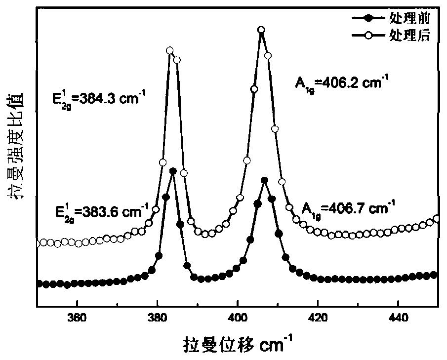
[0052] Usually optical microscope contrast is the most concise and effective method to judge the number of layers of two-dimensional materials, such as figure 1 As shown, the entire MoS before thinning 2 The layer is thicker and the light transmittance is lower. Compared with the sample before treatment, such as figure 2 The sample after the treatment shown has obvious thinning phenomenon, and mo...
Embodiment 2
[0054] This embodiment provides a method for thinning a two-dimensional atomic crystal of a transition metal chalcogenide, the method being:
[0055] Using adhesive tape on MoS 2 The single crystal of the two-dimensional material was repeatedly pasted 5 times, and the sample pasted on the tape was transferred to a silicon wafer coated with an oxide layer on the surface, and the silicon wafer with the sample was soaked in 0.5mmol / L chlorine at 50°C in the gold acid solution for 40 minutes, and then soak the silicon chip in water for 40 minutes to remove the residual moisture on the surface of the silicon chip to obtain the two-dimensional atomic crystal.
[0056] Similar to the evidence in Example 1, the processed samples were Figure 6 , the optical microscope contrast has been improved, such as Figure 7 , the peak difference of Raman characteristic peaks of molybdenum sulfide samples is reduced, such as Figure 8 , the photoluminescence spectral intensity also has a certa...
Embodiment 3
[0058] This embodiment provides a method for thinning a two-dimensional atomic crystal of a transition metal chalcogenide, the method being:
[0059] Use tape to WS 2 The two-dimensional material single crystal was repeatedly pasted 8 times, and the sample pasted on the tape was transferred to a silicon wafer coated with an oxide layer on the surface, and the silicon wafer with the sample was soaked in 0.5mmol / L chlorine at 25°C in the gold acid solution for 30 minutes, and then soak the silicon chip in water for 30 minutes to remove the residual moisture on the surface of the silicon chip to obtain the two-dimensional atomic crystal.
[0060] Similar to the evidence in Example 1, the tungsten sulfide samples before treatment were as Figure 9 It appears yellowish white, because the sample is too thick and has a great reflection effect on the incident light of the optical microscope, so it appears brighter in the grayscale image, while the processed sample is as follows Fig...
PUM
| Property | Measurement | Unit |
|---|---|---|
| thickness | aaaaa | aaaaa |
Abstract
Description
Claims
Application Information


