Plastic semiconductor material and preparation method thereof
An inorganic semiconductor and plastic deformation technology, which is applied in the direction of semiconductor devices, polycrystalline material growth, chemical instruments and methods, etc., can solve the problems of chip peeling performance, high manufacturing cost, and low yield, and achieve strong plastic deformation ability and easy control , The effect of simple process
- Summary
- Abstract
- Description
- Claims
- Application Information
AI Technical Summary
Problems solved by technology
Method used
Image
Examples
Embodiment 1
[0084] Ag 1.8 Cu 0.2 S 0.9 Se 0.1 polycrystalline bulk material
[0085] Mix the elemental raw materials Ag, Cu, S, Se in the glove box according to the molar ratio of 1.8:0.2:0.9:0.1, seal the raw materials into a quartz tube with a carbon film on the inner wall, and use an argon plasma flame to extract the vacuum For packaging, a small amount of Ar gas is filled in the quartz tube for protection. The mixed raw materials were heated to 900°C at a rate of 3°C per minute and melted for 12 hours. Quenching is carried out after melting, and the quenching medium is brine. The ingot obtained by quenching is annealed at 500°C for 100 hours together with the quartz tube, the block is ground into fine powder and then spark plasma sintering is carried out. The sintering temperature is 400°C, the holding time is 2 minutes, and the pressure is 30MPa to obtain Ag. 1.8 Cu 0.2 S 0.9 Se 0.1 Polycrystalline bulk material.
[0086] Tested by the drainage method, showing Ag 1.8 Cu 0...
Embodiment 2
[0088] Ag 2 S semiconductor material crystal ingot
[0089] Mix the elemental raw materials Ag and S in the glove box according to the molar ratio of 2:1, seal the raw materials into a quartz crucible with a pointed bottom, and seal it with an argon plasma flame while drawing a vacuum, and fill the quartz tube with a small amount of Ar gas for protection . The mixed raw materials were melted and cooled at 1000° C. for 12 hours. Afterwards, the quartz tube was put into the crystal descending furnace, the temperature in the constant temperature zone was 830°C, the temperature gradient was 2°C / cm, and the crucible descending speed was 1mm / h to obtain Ag 2 Crystal ingot of S semiconductor material, the photo of which is shown in Figure 10 .
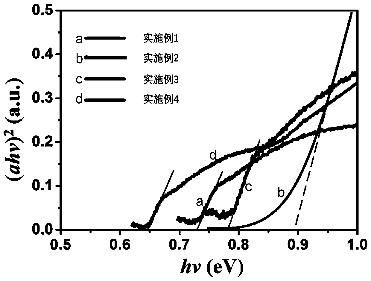
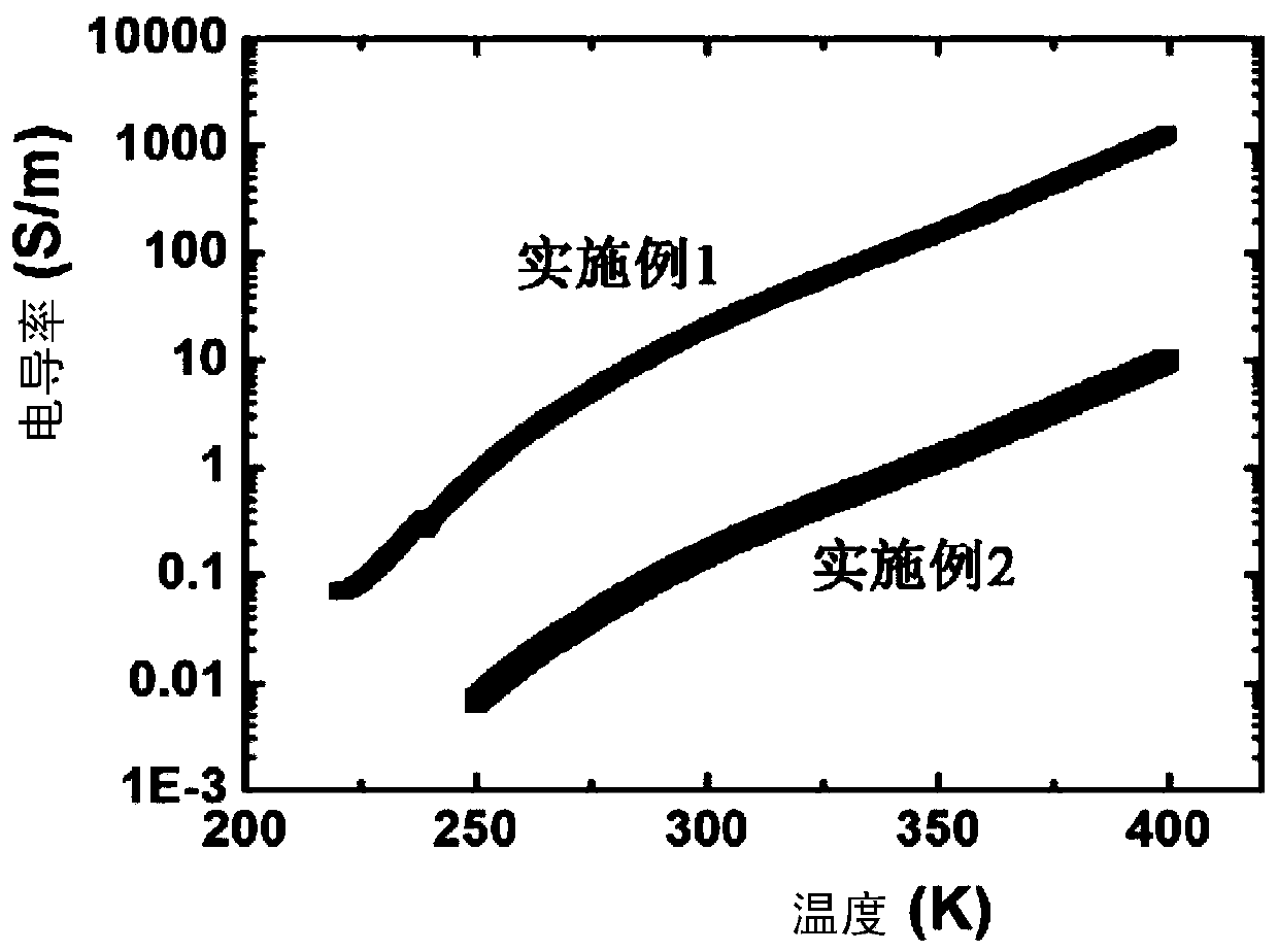
[0090] Tested by spectral absorption method, the band gap is 0.90eV (see figure 2 ). After testing, the room temperature conductivity of the material obtained in Example 2 is 0.15 S / m. The test results of mechanical properties at roo...
Embodiment 3
[0091] Example 3: Ag 1.9 Zn 0.1 S 0.85 I0.15
[0092] Mix the elemental raw materials Ag, Zn, S, and I in the glove box according to the molar ratio of 1.9:0.1:0.85:0.15, seal the raw materials into a quartz tube with a carbon film on the inner wall, and use an argon plasma flame to extract the vacuum For packaging, a small amount of Ar gas is filled in the quartz tube for protection. The mixed raw materials were heated at a rate of 0.5°C per minute to 1000°C for melting for 12 hours. Quenching is carried out after melting, and the quenching medium is brine. The ingot obtained by quenching is annealed at 450°C for 200 hours together with the quartz tube, and the block is ground into fine powder and then subjected to spark plasma sintering. The sintering temperature is 380°C, the holding time is 5 minutes, and the pressure is 40MPa to obtain Ag. 1.9 Zn 0.1 S 0.85 I 0.15 Polycrystalline bulk material.
[0093] Tested by spectral absorption method, the band gap is 0.78eV...
PUM
| Property | Measurement | Unit |
|---|---|---|
| Conductivity | aaaaa | aaaaa |
| Bandgap | aaaaa | aaaaa |
| Conductivity at room temperature | aaaaa | aaaaa |
Abstract
Description
Claims
Application Information
 - R&D Engineer
- R&D Manager
- IP Professional
- Industry Leading Data Capabilities
- Powerful AI technology
- Patent DNA Extraction
Browse by: Latest US Patents, China's latest patents, Technical Efficacy Thesaurus, Application Domain, Technology Topic, Popular Technical Reports.
© 2024 PatSnap. All rights reserved.Legal|Privacy policy|Modern Slavery Act Transparency Statement|Sitemap|About US| Contact US: help@patsnap.com


