A kind of insulator and its preparation method
An insulator and substrate technology, applied in the field of insulating devices and their preparation, can solve the problems of low surface breakdown voltage resistance of insulators, difficult to meet the vacuum insulation requirements of high-voltage devices, poor reliability, etc., so as to reduce surface electric field inhomogeneity and suppress flashing network development, buffering effect of differences in thermal expansion coefficients
- Summary
- Abstract
- Description
- Claims
- Application Information
AI Technical Summary
Problems solved by technology
Method used
Image
Examples
preparation example Construction
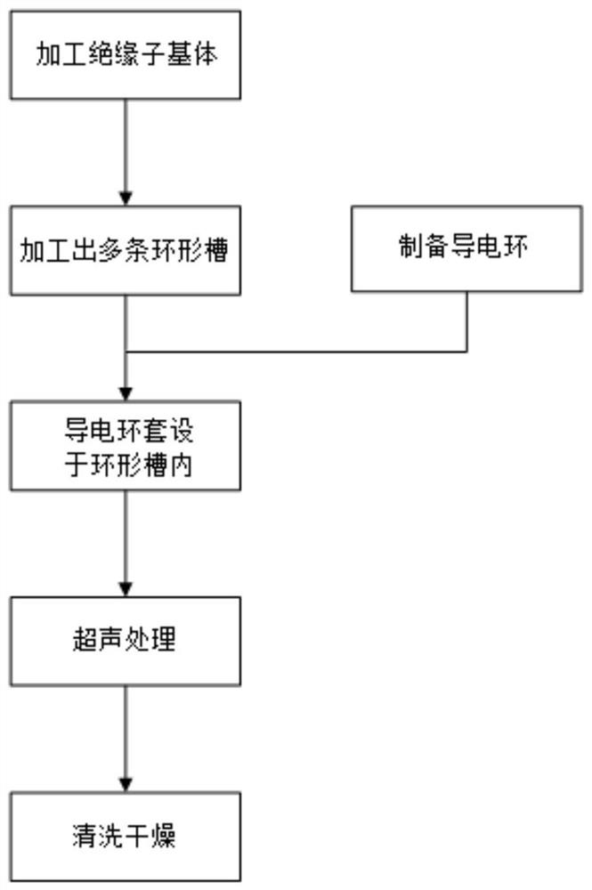
[0037] The preparation method of the above-mentioned insulator is as follows:
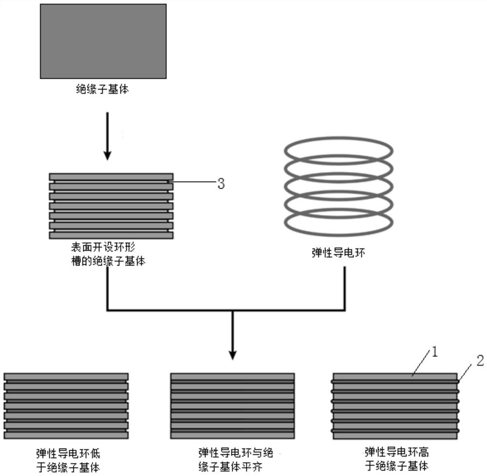
[0038] Step 1, processing to obtain an insulator base 1 . The size of the insulator base 1 is preset according to the usage conditions.
[0039] Step 2, machining a plurality of annular grooves 3 on the surface of the insulator base 1 .
[0040] Step 3, prepare the elastic conductive ring 2 adapted to it according to the size of the annular groove 3, set the elastic conductive ring 2 in the annular groove 3, wherein the inner surface perimeter of the elastic conductive ring 2 in a natural state is larger than the circumference of the annular groove 2%-10% in size. The size of the annular groove 3 here includes the depth, width and circumference of the annular groove 3 , and the size of the elastic conductive ring 2 is prepared to match the annular groove 3 .
[0041] In step 4, the insulator base 1 covered with the elastic conductive ring 2 is ultrasonically treated, cleaned and dried to obtain ...
Embodiment 1
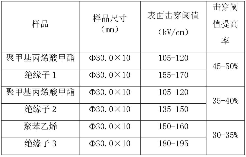
[0045] Polymethyl methacrylate (PMMA) is used as the material of the insulator base 1, and it is processed into a cylindrical insulator of Ф30.0mm×10mm by mechanical processing. After cleaning, it is installed on the rotary table of the carbon dioxide laser. According to the laser parameters, a plurality of annular grooves with an opening width of 0.2 mm, a groove depth of 0.4 mm, and a groove spacing of 0.5 mm are etched on the surface of the insulator substrate 1 . The prepared elastic conductive rings 2 with an inner diameter of 28 mm, a cross-sectional diameter of 0.2 mm, and an electrical conductivity of 0.1 S / cm are sleeved in the annular groove 3 one by one. Finally, the prepared sample is placed in deionized water, ultrasonically oscillated for 1 hour, and the elastic conductive ring 2 is driven to vibrate by ultrasonic waves, releasing the force imbalance caused by uneven local deformation, and finally the elastic conductive ring 2 is lower than the surface of the insu...
Embodiment 2
[0047] Polymethyl methacrylate (PMMA) is used as the material of the insulator base 1, and it is processed into a cylindrical insulator of Ф30.0mm×10mm by mechanical processing. After cleaning, it is installed on the rotary table of the carbon dioxide laser. According to the laser parameters, a plurality of annular grooves with an opening width of 0.4 mm, a groove depth of 0.3 mm, and a groove spacing of 0.5 mm are etched on the surface of the insulator base 1 . The prepared elastic conductive rings 2 with an inner diameter of 28 mm, a cross-sectional diameter of 0.4 mm, and a conductivity of 1 S / cm are set in the annular groove 3 one by one. Finally, the prepared sample is placed in deionized water, ultrasonically oscillated for 1 hour, and the elastic conductive ring 2 is driven to vibrate by ultrasonic waves, releasing the force imbalance caused by uneven local deformation, and finally the elastic conductive ring 2 is higher than the surface of the insulator base 1 The insu...
PUM
| Property | Measurement | Unit |
|---|---|---|
| width | aaaaa | aaaaa |
| depth | aaaaa | aaaaa |
| diameter | aaaaa | aaaaa |
Abstract
Description
Claims
Application Information


