

MOSFET and method for fabricating same
An n-type and p-type technology, applied in the field of device manufacturing, can solve the problems of large switching loss and large on-resistance, and achieve the effects of high applicable voltage, low power consumption, and low energy loss.
- Summary
- Abstract
- Description
- Claims
- Application Information
AI Technical Summary
Problems solved by technology
Method used
Image

Examples
preparation example Construction
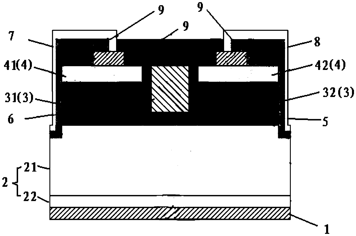
[0061] Another aspect of the present invention provides a method for preparing the above-mentioned MOSFET tube. combine Figure 1-3 , the preparation side of described MOSFET tube comprises the steps:
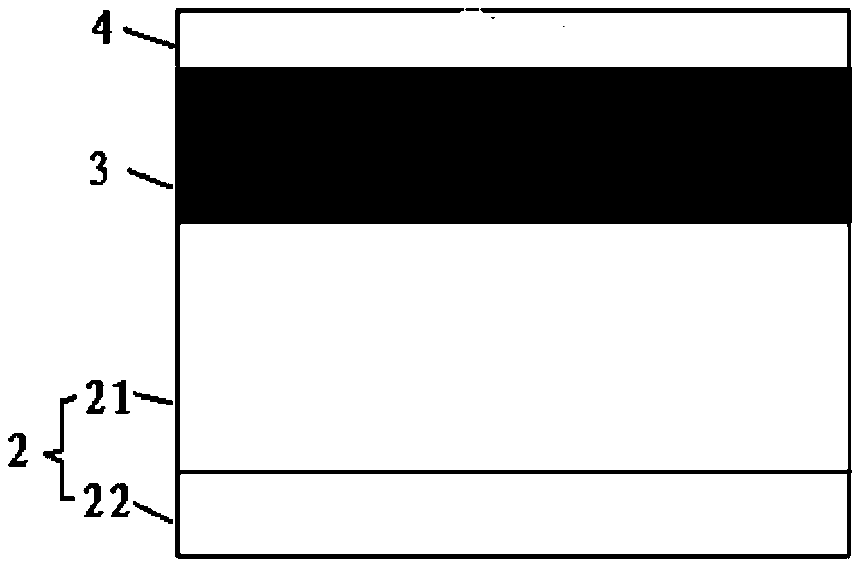
[0062] S01: along the direction extending outward from one surface of the substrate 1, the first n-type Si-doped GaN layer 22, the device drift layer 21, the p-type doped GaN layer 3, the second n-type Si-doped GaN layer 3, and the second Type Si-doped GaN layer 4; formed as figure 2 The layer structure shown.
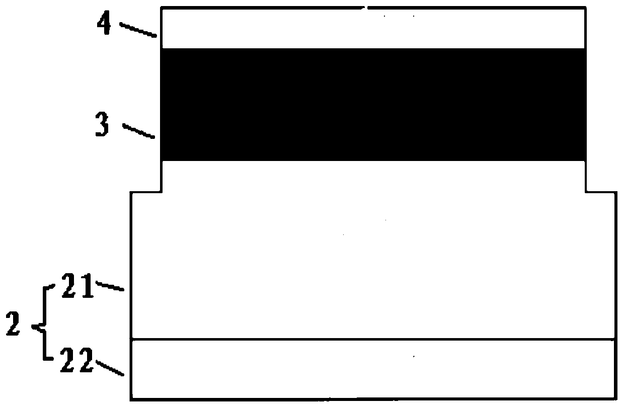
[0063] S02: Etching the edges of the device drift layer 21, the p-type doped GaN layer 3, and the second n-type Si-doped GaN layer 4 to form image 3 The MESA structure shown;
[0064] S03: Etching the middle sections of the p-type doped GaN layer 3 and the second n-type Si-doped GaN layer 4 to form trenches, the trenches penetrating to the surface of the device drift layer 21;
[0065] S04: Depositing a growth gate insulating layer 5 on the inner wall of the tren...
Embodiment 1
[0079] This implementation provides a MOSFET tube, including:
[0080] GaN substrate;
[0081] Substrate, n+-type Si-doped GaN layer thickness 1 μm and lightly Si-doped n-type Si-doped GaN thickness 6 μm;
[0082] The thickness of the P-type Mg-doped GaN layer is 0.3 μm;
[0083] The thickness of the n+ type Si-doped GaN layer is 0.2 μm;
[0084] The thickness of the AlSiO gate insulating layer is 50nm;
[0085] Ti(15nm) / Au(125nm) metal gate;
[0086] Ti(10nm) / Al(240nm) source and Al(250nm) drain;
[0087] SOG field plate dielectric layer;
[0088] This embodiment also provides a preparation method for the MOSFET tube, including:
[0089] Using molecular beam epitaxy (MBE), sequentially grow n+-type Si-doped GaN layers, lightly Si-doped n-type Si-doped GaN layers, p-type Mg-doped GaN layers, n+-type Si-doped GaN layers, and n+-type Si-doped GaN layers on GaN substrates. GaN layer;
[0090] Subsequently, through Cl 2 / SiCl 4 Dry etching on the above layer structure to...
Embodiment 2
[0098] This implementation provides a MOSFET tube, including:
[0099] SiC substrate;
[0100] Substrate, n+-type Si-doped GaN layer thickness 0.4 μm and lightly Si-doped n-type Si-doped GaN thickness 3 μm;
[0101] The thickness of the P-type Mg-doped GaN layer is 0.1 μm;
[0102] The thickness of the n+ type Si-doped GaN layer is 0.1 μm;
[0103] The thickness of the Al2O3 gate insulating layer is 40nm;
[0104] Ti(15nm) / Au(125nm) metal gate;
[0105] Ti(10nm) / Al(240nm) source and Al(250nm) drain;
[0106] SOG field plate dielectric layer;
[0107] This embodiment also provides a preparation method for the MOSFET tube, including:
[0108] Using organic chemical vapor deposition (MOCVD) to sequentially grow n+-type Si-doped GaN layers, lightly Si-doped n-type Si-doped GaN layers, P-type Mg-doped GaN layers, n+-type Si-doped GaN layers, and n+-type Si-doped GaN layers on GaN substrates. Doped GaN layer;
[0109] Subsequently, through Cl 2 / SiCl 4 Dry etching on the a...
PUM
 Abstract
Description
Claims
Application Information