
Communication wave band infrared detector and preparation method thereof

An infrared detector and band technology, applied in the field of detectors, can solve the problems of reducing device sensitivity and response time, Fermi level pinning effect, large dark current and noise, and achieve high mobility and adjustable gate voltage Sexuality, favorable for large-scale preparation and application, fast response effect

Active Publication Date: 2019-08-27
SOUTH CHINA NORMAL UNIVERSITY
View PDF1 Cites 0 Cited by
  • Summary
  • Abstract
  • Description
  • Claims
  • Application Information

AI Technical Summary

Problems solved by technology

However, the hybrid system developed in the past has problems such as the Fermi level pinning effect at the interface, which easily leads to large dark current and noise, and reduces the sensitivity and response time of the device; at the same time, there are no dangling bonds on the surface of the two-dimensional atomic crystal. , so that quantum dots are simply stacked on the surface of a two-dimensional semiconductor, which seriously affects the efficient charge transfer between the two

Method used


Image

  • Communication wave band infrared detector and preparation method thereof
  • Communication wave band infrared detector and preparation method thereof

Examples


Embodiment Construction

[0028] The present invention will be described in further detail below.

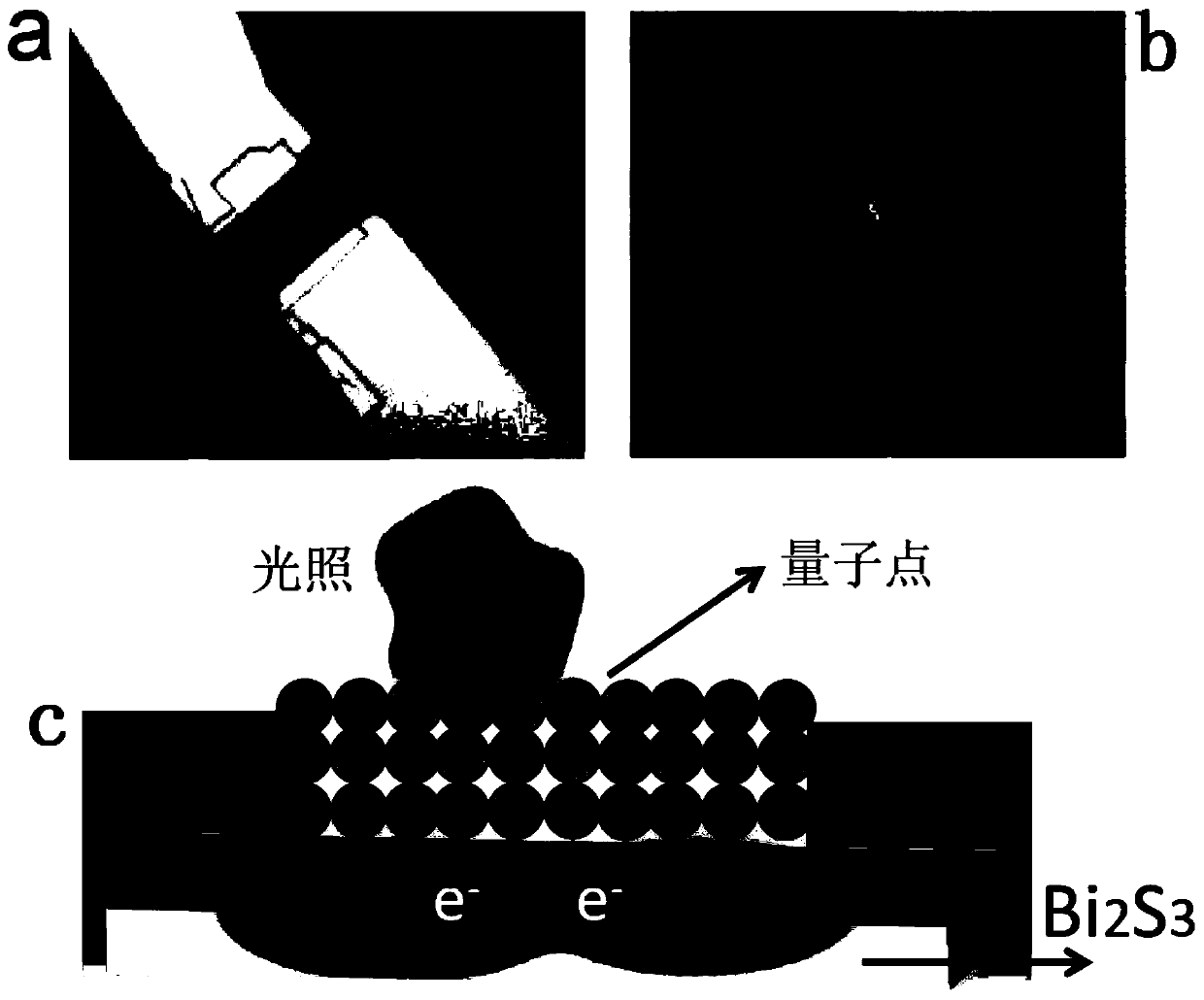
[0029] figure 1 Among them, a contains Bi 2 S 3 The optical microscope image of the infrared detector of the nanosheet, b is the optical microscope image of the infrared detector of the present invention, and c is the structural schematic diagram of the infrared detector of the present invention. Such as figure 1 As shown, the communication band infrared detector of the present invention includes: a substrate, which includes a Si substrate and SiO on the surface of the Si substrate. 2 layer, on SiO 2 Bi on the layer surface 2 S 3 The nanosheet channel layer, located at the Bi 2 S 3 An electrode layer on the surface of the nanoflake channel layer, with openings in the electrode layer exposing the Bi 2 S 3 The surface of the nanoflake channel layer, and the large-sized PbS quantum dot layer grown in the opening, Bi 2 S 3 Due to the large number of surface dangling bonds in the S space on the su...


PUM


Abstract

The invention relates to a communication wave band infrared detector and a preparation method thereof; the infrared detector comprises a Bi2S3 nano sheet channel layer growing on a substrate, an electrode layer growing on the channel layer, and a PbS quantum dot photosensitive layer with a large dimension and growing in an opening, wherein the opening is formed in the electrode layer. The infrareddetector provided by the invention comprises a Bi2S3-PbS mixed system, so that the interface fermi level pinning effect existing in the conventional mixed system can be overcome, the inherent high mobility and the controllability of the gate voltage of the Bi2S3 are kept, and relatively high optical gain and relatively low noise are achieved; the infrared detector disclosed by the invention is wide in spectrum, fast in millisecond magnitude response and high in sensitivity, and can be widely applied to the important fields of optical communication, medical imaging and the like; in addition, the preparation method disclosed by the invention is simple in process, mature in technology, capable of operating at room temperature and low in cost; and the preparation method is very beneficial tolarge-scale preparation and application.

Description

technical field [0001] The invention relates to the field of detectors, in particular to a detector outside the communication band and a preparation method thereof. Background technique [0002] Photoelectric detection technology is the core of many technologies affecting modern human life, which greatly enriches and facilitates people's daily life; especially the communication band infrared detector (due to its advantages of long operating distance, strong penetrating ability, and good anti-interference performance, it is widely used in Military, industrial, medical, security and other fields have extremely extensive and important applications. Although traditional thin film semiconductor (such as InGaAs and InSb) detectors are mature in technology, they also face difficulties in material preparation, complex processes, low temperature work, and cost. Expensive and other problems. Therefore, there is an urgent need to develop new materials and new structures to meet the rap...

Claims


Application Information

Patent Timeline
Patent Type & Authority Applications(China)
IPC IPC(8): H01L31/101H01L31/0352H01L31/02H01L31/18
CPCH01L31/02002H01L31/0352H01L31/035218H01L31/101H01L31/1876Y02P70/50
Inventor 李京波霍能杰刘柳
Owner SOUTH CHINA NORMAL UNIVERSITY
Learn More