Photoelectric detector with graphene sandwich structure

A technology of photodetector and graphene layer, which is applied in the field of photoelectric detection, can solve the problems of small gain and weak signal response ability, and achieve high gain effect, good response effect and high gain detection effect

Active Publication Date: 2019-09-10
CHONGQING INST OF GREEN & INTELLIGENT TECH CHINESE ACADEMY OF SCI
View PDF5 Cites 3 Cited by
  • Summary
  • Abstract
  • Description
  • Claims
  • Application Information

AI Technical Summary

Problems solved by technology

However, like single-band detectors, dual-band detectors based on materials such as mercury cadmium telluride also face the problems of low gain and weak response to weak signals

Method used


Image

  • Photoelectric detector with graphene sandwich structure

Examples


Embodiment 1

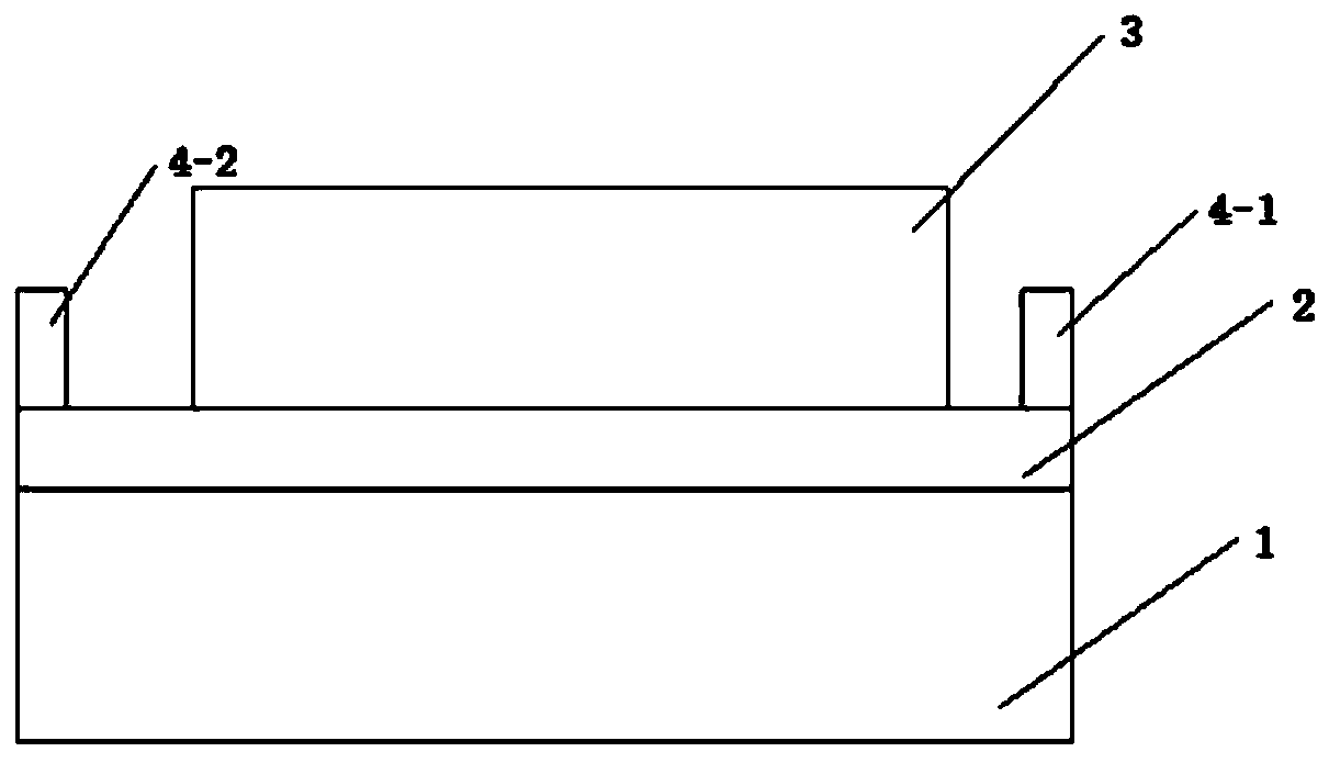
[0036] combined with figure 1 shown. The photodetector comprising the graphene sandwich structure of the present invention includes a light absorbing layer 1 (1), a graphene layer (2), and a light absorbing layer 2 (3) successively from bottom to top, and the graphene layer (2) It is placed between the light-absorbing layer (1) and the light-absorbing layer 2 (3) to form a sandwich structure; the surface of the graphene layer (2) is also provided with a metal electrode (4).

[0037] The material of the light-absorbing layer 1 (1) is a short-wave absorbing material that does not absorb long-wave; the graphene layer (2) provides high-gain carriers for the light-absorbing layer 1 (1) and the light-absorbing layer 2 (3) at the same time transport channel. The material of the light-absorbing layer 1 (1) is a single crystal silicon sheet; the material of the light-absorbing layer 2 (3) is a quantum dot material, preferably a PbS sol-type quantum dot material.

[0038] The photode...

Embodiment 2

[0040] Fabrication method of photodetector

[0041] 1. Preparation of thinned single crystal silicon. Select monocrystalline silicon to be etched to about 10 μm with KOH solution first, then fix the substrate on a quartz substrate spin-coated with polyimide and perform a drying process at about 300 ° C, and then use KOH solution for secondary etching to remove the single crystal The silicon is thinned to a cut-off wavelength absorption thickness of about 1.1 μm.

[0042] 2. Graphene preparation. The graphene film was prepared by chemical vapor deposition equipment, the growth substrate was flat copper foil, and the raw material was analytical pure ethanol. Under the action of high temperature, carbon atoms in ethanol are deposited on the surface of the substrate to form a graphene film after adsorption and migration on the copper substrate. The number of layers of the finally obtained graphene film is controlled at 1-2 layers.

[0043]3. Graphene transfer. The transfer of...


PUM


Abstract

The invention belongs to the technical field of photoelectric detection, and particularly relates to a double-waveband high-gain photoelectric detector with a graphene sandwich structure. The photoelectric detector with the graphene sandwich structure provided by the invention sequentially comprises a light absorption layer I (1), a graphene layer (2) and a light absorption layer II (3) from bottom to top, wherein the graphene layer (2) is arranged between the light absorption layer I (1) and the light absorption layer II (3) to form the sandwich structure; and a metal electrode (4) is arranged on the surface of the graphene layer (2). By virtue of the sandwich structure with unique graphene in combination with the double-layer light absorption material layers, the photoelectric detector can simultaneously respond to light of different wavebands, and a high response effect is obtained; and in addition, the preparation process of the photoelectric detector is simple, and strong in practicability.

Description

technical field [0001] The invention belongs to the technical field of photoelectric detection, in particular to a dual-band high-gain photoelectric detector including a graphene interlayer structure. Background technique [0002] Photoelectric detection technology is the reproduction and expansion of the human eye. Using photoelectric detectors such as ultraviolet and infrared, it can achieve imaging effects that the human eye cannot achieve in special environments such as night. However, photodetection in a single band has its own limitations. For example, although infrared detection has the advantages of breaking through the limits of the human eye and realizing night vision functions, it also has the disadvantage of not conforming to the visual habits of imaging; although visible light detection has the advantage of matching the imaging habits of the human eye, it cannot detect infrared and night targets. Wait. So the researchers thought that by using image fusion tech...

Claims


Application Information

Patent Timeline
Patent Type & Authority Applications(China)
IPC IPC(8): H01L31/101H01L31/11H01L31/18
CPCH01L31/1013H01L31/11H01L31/18Y02P70/50
Inventor 申钧吴启明魏兴战冯双龙周大华汤林龙冷重钱聂长斌张之胜伍俊史浩飞
Owner CHONGQING INST OF GREEN & INTELLIGENT TECH CHINESE ACADEMY OF SCI
Why Eureka
Try Eureka