A photodetector comprising a graphene sandwich structure
A photodetector and graphene layer technology, applied in the field of photoelectric detection, can solve the problems of weak signal response ability and small gain, etc., and achieve the effects of good response effect, high gain effect, and high gain detection effect.
- Summary
- Abstract
- Description
- Claims
- Application Information
AI Technical Summary
Problems solved by technology
Method used
Image
Examples
Embodiment 1
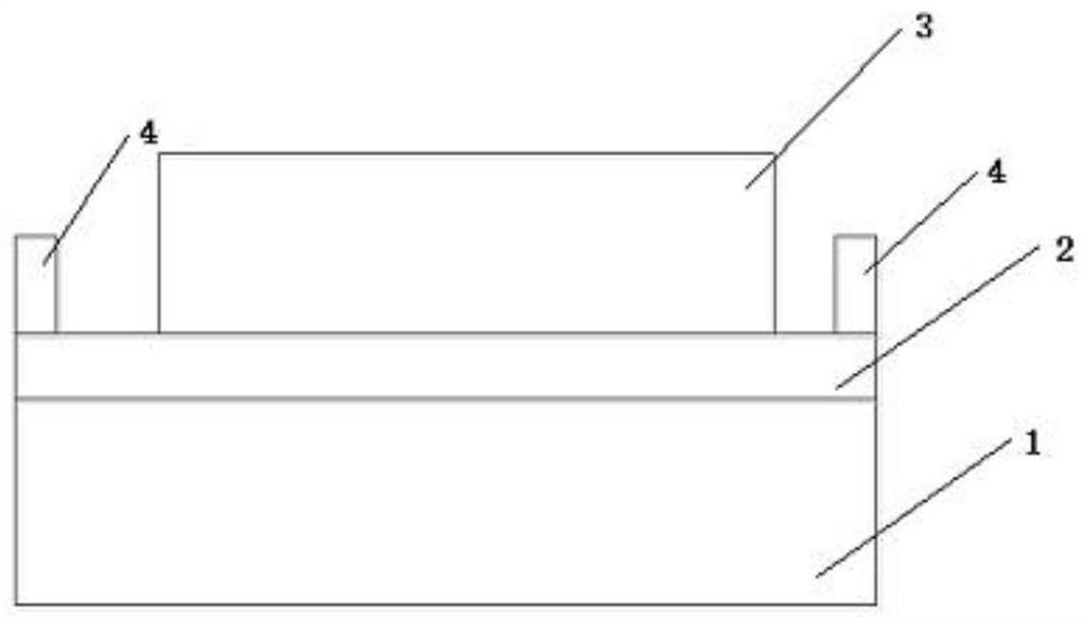
[0036] combined with figure 1 shown. The photodetector comprising the graphene sandwich structure of the present invention includes a first light absorption layer 1, a graphene layer 2, and a second light absorption layer 3 from bottom to top, and the graphene layer 2 is placed in the first light absorption layer. Between the layer 1 and the second light absorbing layer 3, a sandwich structure is formed; the surface of the graphene layer 2 is also provided with a metal electrode (4).
[0037] The material of the first light-absorbing layer 1 is a short-wave absorbing material, which does not absorb long-wave; the graphene layer 2 simultaneously provides a high-gain carrier transport channel for the first light-absorbing layer 1 and the second light-absorbing layer 3 . The material of the first light-absorbing layer 1 is a single crystal silicon sheet; the material of the second light-absorbing layer 3 is a quantum dot material, preferably a PbS sol-type quantum dot material. ...
Embodiment 2
[0040] Fabrication method of photodetector
[0041] 1. Preparation of thinned single crystal silicon. Select monocrystalline silicon to be etched to about 10 μm with KOH solution first, then fix the substrate on a quartz substrate spin-coated with polyimide and perform a drying process at about 300 ° C, and then use KOH solution for secondary etching to remove the single crystal The silicon is thinned to a cut-off wavelength absorption thickness of about 1.1 μm.
[0042] 2. Graphene preparation. The graphene film was prepared by chemical vapor deposition equipment, the growth substrate was flat copper foil, and the raw material was analytical pure ethanol. Under the action of high temperature, carbon atoms in ethanol are deposited on the surface of the substrate to form a graphene film after adsorption and migration on the copper substrate. The number of layers of the finally obtained graphene film is controlled at 1-2 layers.
[0043]3. Graphene transfer. The transfer of...
PUM
| Property | Measurement | Unit |
|---|---|---|
| thickness | aaaaa | aaaaa |
| wavelength | aaaaa | aaaaa |
| thickness | aaaaa | aaaaa |
Abstract
Description
Claims
Application Information
 - R&D
- Intellectual Property
- Life Sciences
- Materials
- Tech Scout
- Unparalleled Data Quality
- Higher Quality Content
- 60% Fewer Hallucinations
Browse by: Latest US Patents, China's latest patents, Technical Efficacy Thesaurus, Application Domain, Technology Topic, Popular Technical Reports.
© 2025 PatSnap. All rights reserved.Legal|Privacy policy|Modern Slavery Act Transparency Statement|Sitemap|About US| Contact US: help@patsnap.com

