Silicon microphone and processing method thereof

A technology for silicon microphones and substrates, applied in loudspeakers, electrostatic transducers, microphones, sensors, etc., can solve problems such as solder slag damage to MEMS acoustic-electric conversion chips, insufficient bonding strength of conductive adhesive, and decline in the yield of silicon microphones. , to achieve the effects of structural stability and yield, minimization of size, minimization of support strength temperature and thickness

Pending Publication Date: 2019-09-17
SUZHOU JIEYANXIN NANO TECH CO LTD
View PDF0 Cites 10 Cited by
  • Summary
  • Abstract
  • Description
  • Claims
  • Application Information

AI Technical Summary

Problems solved by technology

[0005] One is to directly use conductive adhesive to bond the metal shell and the circuit board substrate together. This technology can achieve better electrical connection, but the bonding strength of the conductive adhesive is not enough, which may easily lead to insufficient mechanical strength of the product.
[0006] Another way is to use conductive solder paste to weld the metal shell and the circuit board substrate together. This technology can achieve a bette...

Method used


Image

  • Silicon microphone and processing method thereof
  • Silicon microphone and processing method thereof
  • Silicon microphone and processing method thereof

Examples


Embodiment Construction

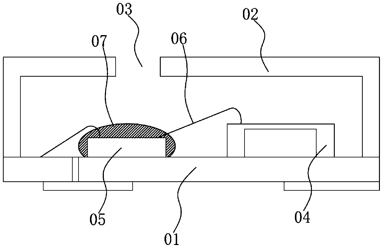
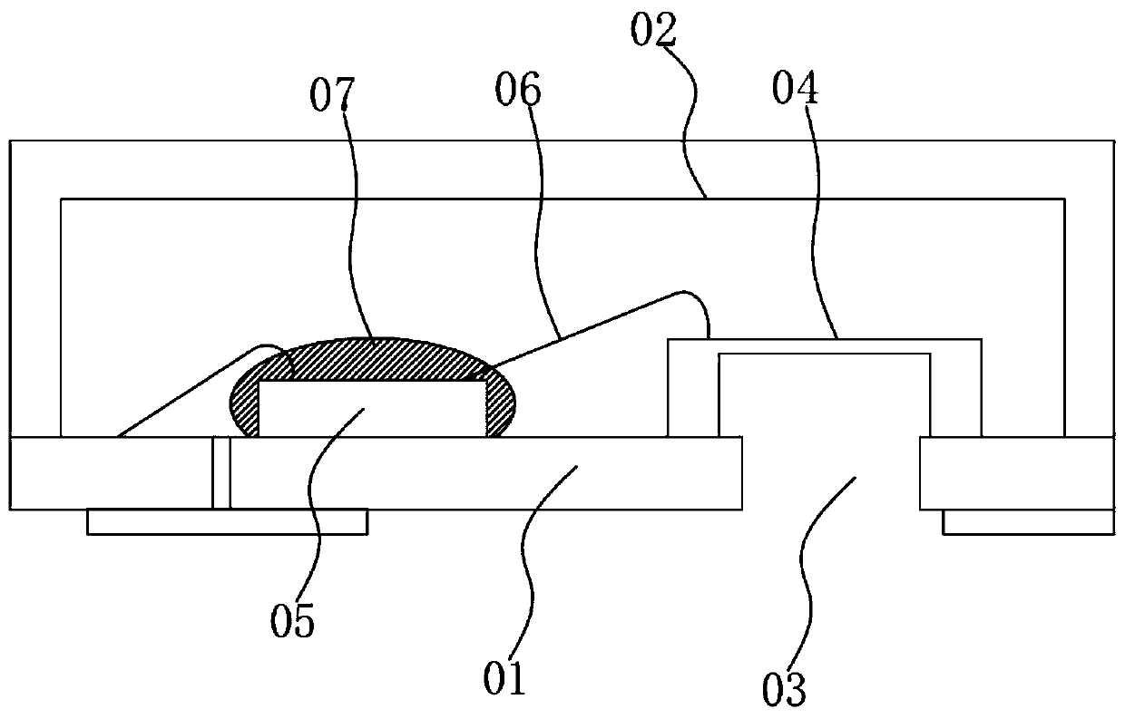
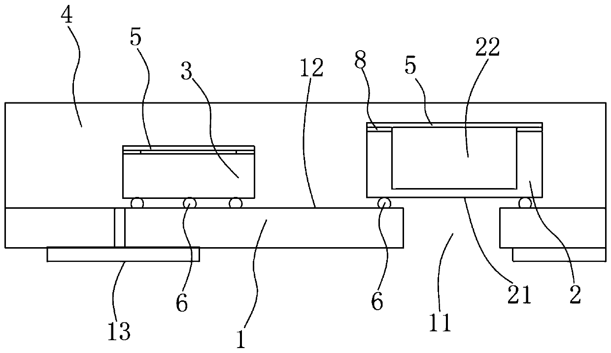
[0050] Objects, advantages and features of the present invention will be illustrated and explained by the following non-limiting description of preferred embodiments. These embodiments are only typical examples of applying the technical solutions of the present invention, and all technical solutions formed by adopting equivalent replacements or equivalent transformations fall within the protection scope of the present invention.

[0051] In the description of the scheme, it should be noted that the terms "center", "upper", "lower", "left", "right", "front", "rear", "vertical", "horizontal", " The orientation or positional relationship indicated by "inner", "outer", etc. is based on the orientation or positional relationship shown in the drawings, and is only for the convenience of description and simplification of description, rather than indicating or implying that the device or element referred to must have a specific orientation , constructed and operated in a particular or...


PUM

PropertyMeasurementUnit
Thicknessaaaaaaaaaa

Abstract

The invention discloses a silicon microphone and a processing method thereof. The silicon microphone comprises a circuit board substrate, an MEMS sound pressure sensing chip and an ASIC chip. The circuit board substrate is provided with a sound inlet hole which is right opposite to an induction area of the MEMS sound pressure sensor chip, wherein the MEMS sound pressure sensing chip and the ASIC chip are in inverted interconnection with the circuit board substrate and are wrapped in the thermosetting plastic film layer, and the thermosetting plastic film layer is fixedly connected with the circuit board substrate and covers the chip mounting surface of the circuit board substrate. According to the scheme, the conventional thinking mode that the silicon microphone is packaged by the metal shell is changed; the MEMS sound pressure sensing chip and the ASIC chip are wrapped by a thermosetting plastic film. Compared with the prior art, the structure of a metal shell is omitted, the size of a device is greatly reduced, meanwhile, the connection stability of the thermosetting plastic film layer and the circuit board substrate is higher than that of a conventional conductive adhesive, welding operation is not needed, the problem of chip pollution possibly generated in the welding process is avoided, and the combination of the structural stability of a product and the improvement of the yield is effectively achieved.

Description

technical field [0001] The invention relates to the field of packaging of electronic products, in particular to a silicon microphone and a processing method thereof. Background technique [0002] As mobile phones, notebooks, hearing aids, headsets and other electronic products have smaller and smaller size requirements for internal parts, a large number of smaller and better quality silicon microphones are used. Silicon microphones, also known as MEMS microphones, are manufactured based on MEMS technology. Microphone, composed of MEMS boost sensor chip, ASIC chip, sound cavity and RF suppression circuit. The MEMS sound pressure sensor is a miniature capacitor composed of a silicon diaphragm and a silicon back plate, which can convert the sound pressure change into a capacitance change, and then convert the ASIC chip capacitance change into an electrical signal to realize "sound-to-sound" conversion . [0003] Most existing silicon microphones include packages such as attac...

Claims


Application Information

Patent Timeline
IPC IPC(8): H04R19/04H04R31/00
CPCH04R19/04H04R31/003H04R2201/003H04R2231/001
Inventor 王建国申亚琪
Owner SUZHOU JIEYANXIN NANO TECH CO LTD
Why Eureka
Try Eureka