cis gene chip and its making method

A technology of a gene chip and a production method, which is applied to the field of CIS gene chip and its production, can solve the problems of low sensitivity, large size of the test instrument, and reduce the test accuracy rate, so as to improve the accuracy rate, improve the signal sensitivity, and improve the mass production. degree of effect

Active Publication Date: 2022-08-09
WUHAN XINXIN SEMICON MFG CO LTD
View PDF7 Cites 0 Cited by
  • Summary
  • Abstract
  • Description
  • Claims
  • Application Information

AI Technical Summary

Problems solved by technology

[0004] However, there are various problems in the existing gene chip and detection, for example: the gene chip requires a specific test and analysis instrument, and the test instrument is large in size; the sample is detected by the photoelectric signal, the analysis time is long and the optical signal crosstalk It will reduce the test accuracy; the mass production of gene chips is low; the sensitivity of detection of gene chip samples is low

Method used


Image

  • cis gene chip and its making method
  • cis gene chip and its making method
  • cis gene chip and its making method

Examples


Embodiment Construction

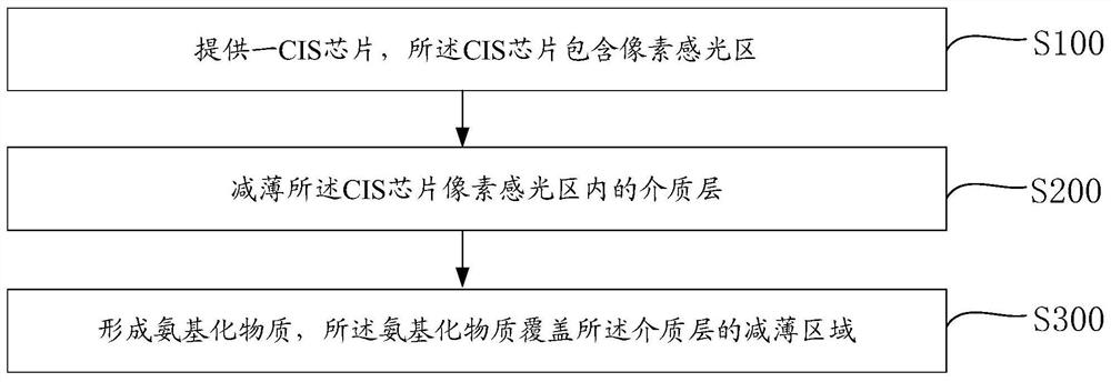
[0035] Based on the above problems, the present invention provides a method for manufacturing a CIS (CMOS Image Sensor, CMOS image sensor) gene chip, including: providing a CIS chip, the CIS chip including a pixel photosensitive area, and thinning the pixel photosensitive area of ​​the CIS chip a dielectric layer within, and an amined species is formed that covers the thinned region of the dielectric layer.

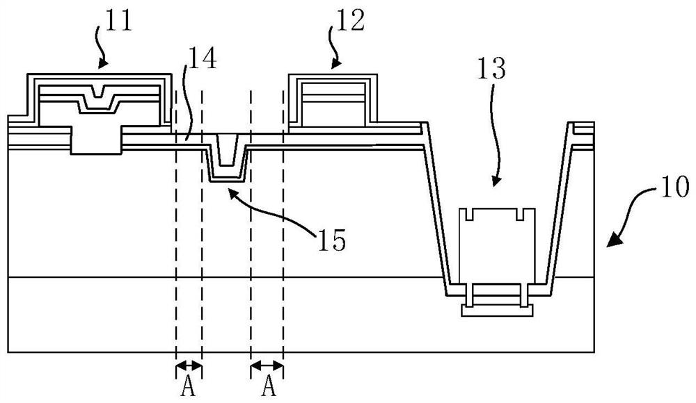
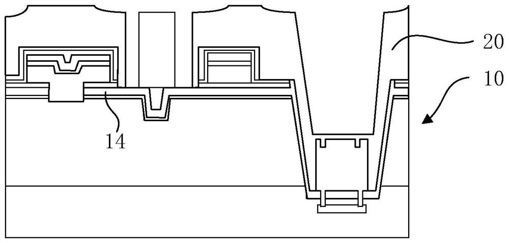
[0036] Correspondingly, the present invention also provides a CIS gene chip, comprising: a CIS chip, the CIS chip includes a pixel photosensitive region, and the thickness of the dielectric layer in the pixel photosensitive region is smaller than the thickness of the dielectric layer in the remaining regions, and Aminated substances, the aminated substances are located on the relatively thin dielectric layer in the pixel photosensitive region.

[0037] In the CIS gene chip and the manufacturing method thereof provided by the present invention, the dielectric layer in the ...


PUM


Abstract

The invention provides a CIS gene chip and a manufacturing method thereof. The method includes: providing a CIS chip, the CIS chip includes a pixel photosensitive area, thinning a dielectric layer in the pixel photosensitive area of ​​the CIS chip; forming an amination The aminated substance covers the thinned area of ​​the dielectric layer, and the CIS gene chip formed thereby can shorten the distance between the signal source and the signal collection area, improve the signal sensitivity, and improve the accuracy of the test results. At the same time, its analysis equipment can be miniaturized, and it can break the site limitation of gene analysis and reduce the cost, and can improve the mass production of CIS gene chips.

Description

technical field [0001] The invention relates to the technical field of semiconductor manufacturing, in particular to a CIS gene chip and a manufacturing method thereof. Background technique [0002] Gene chips use a large number of specific oligonucleotide fragments or gene fragments as probes, which are regularly fixed on solid supports such as silicon wafers, glass wafers, plastic wafers or nylon substrates combined with photoelectric measuring devices to form a two-dimensional The array is hybridized with the gene of the labeled sample to be tested according to the principle of base pairing, thereby detecting a specific gene. [0003] Gene probe utilizes hydrogen bonding between complementary bases of ribose double-strand to form a stable double bond structure, and detects the sample by measuring the photoelectric signal on the target gene, thus making gene chip technology an efficient large-scale acquisition. important means of relevant biological information. [0004]...

Claims


Application Information

Patent Timeline
Patent Type & Authority Patents(China)
IPC IPC(8): C40B40/06C40B50/18
CPCC40B40/06C40B50/18Y02P70/50
Inventor 叶国梁刘天建占迪
Owner WUHAN XINXIN SEMICON MFG CO LTD
Why Eureka
Try Eureka