
An electronic equipment housing and electronic equipment
A technology for electronic equipment and shells, which is applied in the field of electronic equipment shells and electronic equipment, can solve problems such as cracking of coating layers, achieve the effects of reducing thermal expansion coefficient, solving cracking of coating layers, and improving dimensional thermal stability
- Summary
- Abstract
- Description
- Claims
- Application Information
AI Technical Summary
Problems solved by technology
Method used
Image

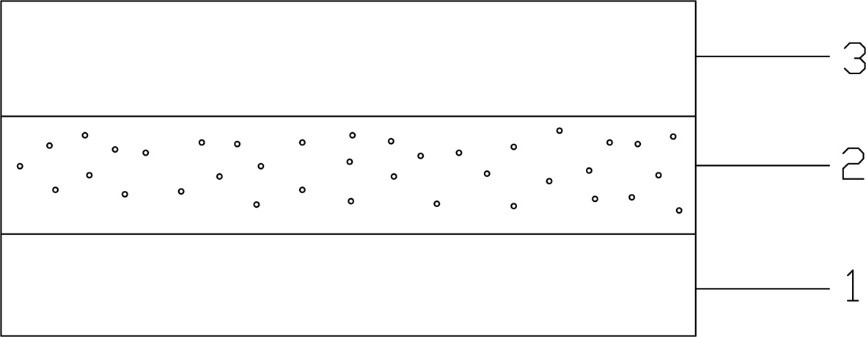
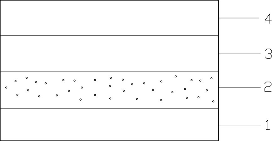
Examples
Embodiment 1
[0033] A layer of UV-curable adhesive containing zirconium dioxide was applied on the surface of polymethyl methacrylate (thickness 0.05 mm) and polycarbonate (thickness 0.3 mm) double-layer transparent polymer substrate using a transfer printing machine Particles (average particle size is 40nm), the weight of zirconia particles is 8% of the weight of UV curing glue; under the action of UV light, the UV curing glue is polymerized and cured to form a texture layer with a certain shape (thickness is 7 μm) ; Deposit titanium nitride and silicon dioxide coating layers on the surface of the texture layer (total thickness is 100 nm), the coating can reflect blue light with a central wavelength of 450 nm; heat press the polymer matrix treated above to obtain electronic equipment shells Body S1.
Embodiment 2
[0035] Use a transfer machine to coat a layer of UV-curable adhesive on the surface of polymethyl methacrylate (thickness 0.05 mm) and polycarbonate (thickness 0.5 mm) double-layer transparent polymer substrate, which contains silica Particles (average particle size 20nm), the weight of silica particles is 25% of the weight of the UV curable adhesive; under the action of UV light, the UV curable adhesive is polymerized and cured to form a textured layer with a certain shape (thickness 15 μm) ; Deposit titanium dioxide and silicon dioxide coating layers (total thickness 50 nm) on the surface of the texture layer, and the coating can reflect blue light with a center wavelength of 450 nm; print an ink layer (thickness 15 μm) on the surface of the coating layer, which will pass through the above The treated polymer matrix is thermocompressed to obtain an electronic device casing S2.
Embodiment 3
[0037] A three-layer transparent polymer substrate of polymethyl methacrylate (thickness 0.05 mm), polycarbonate (thickness 0.5 mm) and polymethyl methacrylate (thickness 0.05 mm) was coated with a transfer printing machine. A layer of UV curable adhesive, containing silica particles (average particle size 30 nm) in the UV curable adhesive, the weight of the silica particles is 40% of the weight of the UV curable adhesive; the UV curable adhesive is polymerized and cured under the action of UV light, Form a texture layer with a certain shape (thickness is 30 μm); deposit titanium dioxide and silicon dioxide coating layers on the surface of the texture layer (total thickness is 50 nm), the coating can reflect blue light with a central wavelength of 450 nm; on the coating layer An ink layer (thickness: 30 μm) was printed on the surface, and the above-mentioned treated polymer matrix was thermocompressed to obtain the electronic device casing S3.
PUM
| Property | Measurement | Unit |
|---|---|---|
| The average particle size | aaaaa | aaaaa |
| Thickness | aaaaa | aaaaa |
| Thickness | aaaaa | aaaaa |
Abstract
Description
Claims
Application Information