Repair method of single crystal/directional solidified nickel-based high-temperature alloy and application of repair method
A nickel-based superalloy, directional solidification technology, applied in the field of metal processing, can solve problems such as easy cracking and inability to obtain continuous directional growth structure, and achieve the effects of ensuring the suppression of thermal cracks, shortening the production cycle, and suppressing the generation of thermal cracks
- Summary
- Abstract
- Description
- Claims
- Application Information
AI Technical Summary
Problems solved by technology
Method used
Image
Examples
Embodiment 1
[0060] Table 1 The composition of the alloy to be repaired in Example 1 of the present invention (wt%)
[0061]
[0062] In this embodiment, parts with alloy compositions shown in Table 1 are repaired, and the parts to be repaired and the laser deposition powder are of the same material.
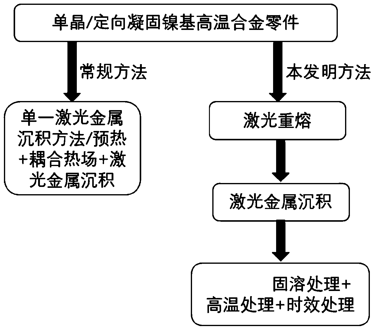
[0063] Step 1: Perform laser remelting treatment on the wound of the part to be repaired to form a transition layer: the laser remelting power is 130W, the scanning rate is 4mm / s, the laser spot diameter is 3mm, the scanning pass spacing is 0.3mm, and the laser wavelength is 1064nm , the alloy parts have been air-cooled to room temperature before the start of each pass. The thickness of the transition layer is 120 μm.
[0064] Step 2: Carry out laser metal deposition treatment on the transition layer, the peak power is 800W, the peak-valley power is 50W, the peak power is 6ms each time, and the peak-valley power is 4ms each time, alternately (see Figure 4 ), the laser power is 100Hz; t...
Embodiment 2
[0069] The unexplained parts adopt the same method and conditions as in Example 1.
[0070] The laser remelting power is 100W, the scanning speed is 4mm / s, the laser spot diameter is 3mm, the scanning pass spacing is 0.3mm, and the laser wavelength is 1064nm. Alloy parts have been air-cooled to room temperature before the start of each pass. The thickness of the transition layer is 110 μm. Laser metal deposition treatment, the peak power is 800W, the peak-valley power is 100W, the peak power is 2ms each time, the peak-valley power is 8ms each time, alternately, the laser power is 100Hz; the powder feeding amount is 7.2g / min, the carrier gas voltage is 4V, the particle size is 300 mesh, the scanning speed is 4mm / s, the laser spot diameter is 3mm, and the laser wavelength is 1064nm. The scanning strategy is a bidirectional scanning path, the scanning pass interval is 0.5 mm, the alloy parts have been air-cooled to room temperature before each pass, and the deposition layer he...
Embodiment 3
[0073] The unexplained parts adopt the same method and conditions as in Example 1.
[0074] The laser remelting power is 150W, the scanning speed is 12mm / s, the laser spot diameter is 3mm, the scanning pass spacing is 0.5mm, and the laser wavelength is 1064nm. Alloy parts have been air-cooled to room temperature before the start of each pass. The thickness of the transition layer is 50 μm. Laser metal deposition treatment, the peak power is 1200W, the peak-valley power is 150W, the peak power is 6ms each time, the peak-valley power is 4ms each time, alternately, the laser power is 100Hz; the powder feeding amount is 12g / min , the carrier gas voltage is 3.8V, the particle size is 100 mesh, the scanning speed is 12mm / s, the laser spot diameter is 3mm, and the laser wavelength is 1064nm. The scanning strategy is a bidirectional scanning path, the scanning pass interval is 0.5 mm, the alloy parts have been air-cooled to room temperature before each pass, and the deposition layer...
PUM
 Abstract
Description
Claims
Application Information


