SiC MOSFET power device and preparation method thereof
A technology of power devices and trenches, which is applied in the direction of semiconductor devices, electrical components, circuits, etc., can solve the problems of power module overall size and economic cost increase, long reverse recovery time, poor reverse conduction characteristics, etc., to reduce the overall Effects of size and economic cost, reduction of electric field strength, and reduction of reverse conduction voltage drop
- Summary
- Abstract
- Description
- Claims
- Application Information
AI Technical Summary
Problems solved by technology
Method used
Image
Examples
Embodiment 1
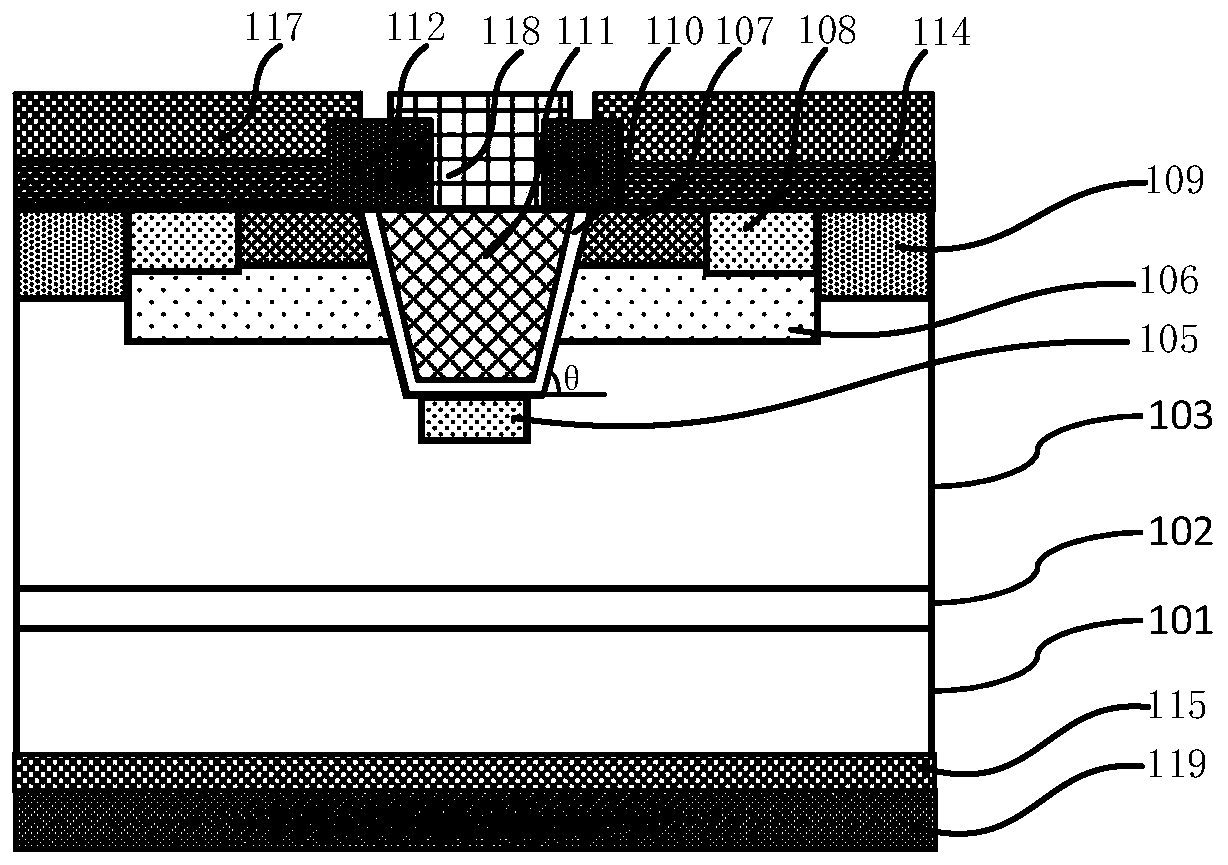
[0086] Such as figure 1 As shown, the present invention provides a SiC MOSFET power device, including: a substrate 101 of a first conductivity type; an epitaxial layer 103 of the first conductivity type located on the surface of the substrate 101, the epitaxial layer 103 and the The material of the substrate 101 includes SiC; the trench 104 ( figure 1 Not marked in), located in the epitaxial layer 103, the upper opening of the trench 104 is larger than the lower opening so that the trench 104 has an inclined slope; the gate dielectric layer 110 is located on the side of the trench 104 The wall and bottom surface; the gate conductive layer 111 is located on the surface of the gate dielectric layer 110 and fills the trench 104; the well region 106 of the second conductivity type is located in the epitaxial layer 103 and is located in the trench On the periphery of the trench 104, the second conductivity type is different from the first conductivity type; the source region 107 of t...
Embodiment 2
[0099] Such as Figure 2 to Figure 13 As shown, the present invention also provides a method for preparing a SiC MOSFET power device, which can be used to prepare the SiC MOSFET power device in the first embodiment, so the description of the SiC MOSFET power device in the first embodiment is fully applicable to this embodiment For example, similarly, the description of the same structure in this embodiment also applies to the first embodiment. For the sake of brevity, this embodiment will minimize repetitive introductions. For details, please refer to the description in Embodiment 1.
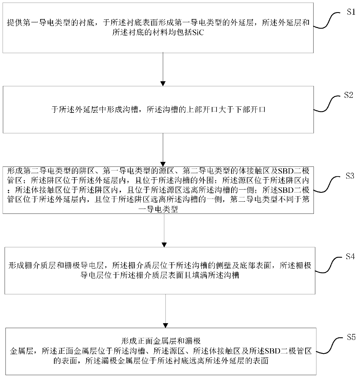
[0100] Please refer to figure 2 , The preparation method includes the steps:
[0101] S1: Provide a substrate 101 of the first conductivity type, and form an epitaxial layer 103 of the first conductivity type on the surface of the substrate 101, and the materials of the epitaxial layer 103 and the substrate 101 both include SiC;
[0102] S2: forming a trench 104 in the epitaxial layer 103, the upper ...
PUM
| Property | Measurement | Unit |
|---|---|---|
| thickness | aaaaa | aaaaa |
| depth | aaaaa | aaaaa |
| width | aaaaa | aaaaa |
Abstract
Description
Claims
Application Information


