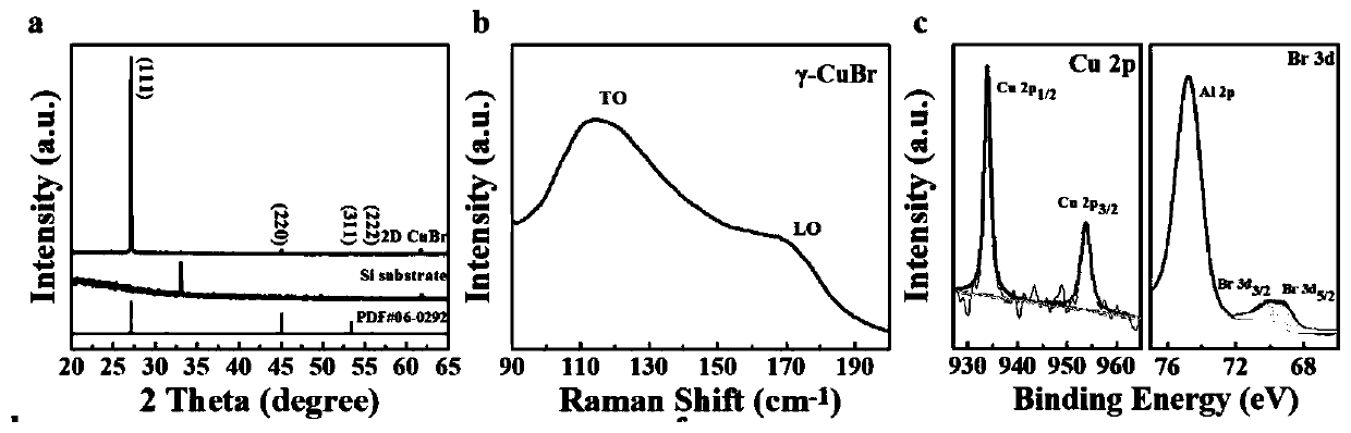
Preparation method and application of two-dimensional ultra-thin CuBr nano sheet
An ultra-thin, single-crystal nanotechnology, applied in nanotechnology, nanotechnology, chemical instruments and methods, etc., can solve the problems of good CuBr single crystal, difficult to prepare high-quality two-dimensional non-layered CuBr single crystal materials, etc. To achieve the effect of easy control of process parameters, high yield and strong controllability
- Summary
- Abstract
- Description
- Claims
- Application Information
AI Technical Summary
Problems solved by technology
Method used
Image


Examples
Embodiment 1
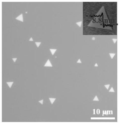
[0030] A preparation method of a two-dimensional ultrathin CuBr single crystal nanosheet, comprising the following steps:
[0031] Step 1: Add 10 mg of BiBr 3 powder on Al 2 o 3 Crucible, then put the crucible into the center of the first heating zone upstream of the quartz tube; place the mica substrate on the quartz plate, cover the copper foil with a flat surface on the substrate, control the distance between the copper foil and the mica substrate to be 50 μm, and then place the The quartz plate is placed in the center of the second heating zone downstream of the quartz tube;
[0032] Step 2: Vacuumize the inside of the quartz tube to below 0.1Pa, and pass 500 sccm of Ar gas to remove the residual air in the tube and keep the air pressure in the tube at normal pressure, and then pass H into the tube 2 5% Ar / H by volume 2 Mixed gas, adjust the air flow to the flow rate required for material growth of 50 sccm;
[0033] Step 3: Heat the second heating zone to 325°C within...
Embodiment 2
[0037] A preparation method of a two-dimensional ultrathin CuBr single crystal nanosheet, comprising the following steps:
[0038] Step 1: Add 10 mg of BiBr 3 powder on Al 2 o 3 Put the crucible into the center of the first heating zone upstream of the quartz tube; place the mica substrate on the quartz plate, cover the substrate with flat copper foil, and control the distance between the copper foil and the mica substrate to be 0 μm, and then place the The quartz plate is placed in the center of the second heating zone downstream of the quartz tube;
[0039] Step 2: Vacuumize the inside of the quartz tube to below 0.1Pa, and pass 500 sccm of Ar gas to remove the residual air in the tube and keep the air pressure in the tube at normal pressure, and then pass H into the tube 2 5% Ar / H by volume 2 Mixed gas, adjust the air flow to the flow rate required for material growth of 50 sccm;
[0040] Step 3: Heat the second heating zone to 325°C within 15 minutes, keep it for 15 m...
Embodiment 3
[0043] Step 1: Add 50 mg of BiBr 3 powder on Al 2 o 3Then put the crucible into the center of the first heating zone upstream of the quartz tube, place the mica substrate on the quartz plate, cover the substrate with flat copper foil, control the distance between the copper foil and the mica substrate to be 25 μm, and then place the The quartz plate is placed in the center of the second heating zone downstream of the quartz tube;
[0044] Step 2: Vacuumize the inside of the quartz tube to below 0.1Pa, and introduce 500 sccm of Ar gas to remove the residual air in the tube and keep the air pressure in the tube at normal pressure, and then inject Ar gas into the tube to adjust the air flow to the growth of the material The required flow rate is 75 sccm;
[0045] Step 3: Heating the second heating zone to 305°C within 15 minutes, keeping it for 15 minutes, then heating the first heating zone to 275°C within 10 minutes, reacting for 5 minutes, cooling naturally to room temperat...
PUM
| Property | Measurement | Unit |
|---|---|---|
| thickness | aaaaa | aaaaa |
| thickness | aaaaa | aaaaa |
| size | aaaaa | aaaaa |
Abstract
Description
Claims
Application Information