Phononic crystal-based film bulk acoustic resonator
A thin-film bulk acoustic wave and phononic crystal technology, which is applied in the field of resonators, can solve the problems of inability to reflect transverse shear waves, low device quality factor, and inability to reflect longitudinal waves, so as to reduce losses, reduce transverse shear waves, The effect of improving power capacity
- Summary
- Abstract
- Description
- Claims
- Application Information
AI Technical Summary
Problems solved by technology
Method used
Image
Examples
Embodiment 1
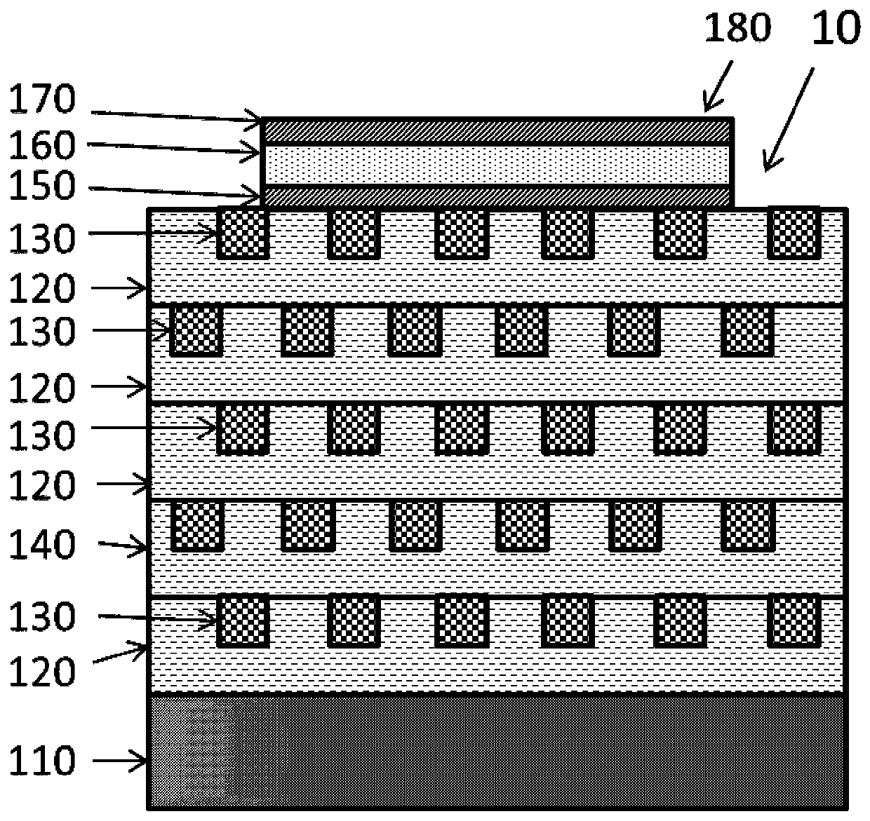
[0022] Such as figure 1 As shown, the thin-film bulk acoustic resonator 10 based on phononic crystals of the present invention includes a substrate 110, the substrate material is high-resistance silicon; it includes a phononic crystal layer 140 formed on the front side of the substrate, formed on the phononic crystal The piezoelectric oscillator stack structure 180 on the layer 140; wherein the phononic crystal layer includes multiple layers of phononic crystals arranged periodically, and each layer of phononic crystals is arranged alternately and periodically with scatterers and substrates of different materials, such as scatterers 130 The material can be silicon dioxide, air and other low-sonic materials, and the material of the substrate 120 can be high-sonic materials such as tungsten, high-resistance silicon, and aluminum nitride; in this embodiment, the scatterer structure in the phononic crystal is a cuboid, The matrix structure is also a cuboid; in the present inventio...
Embodiment 2
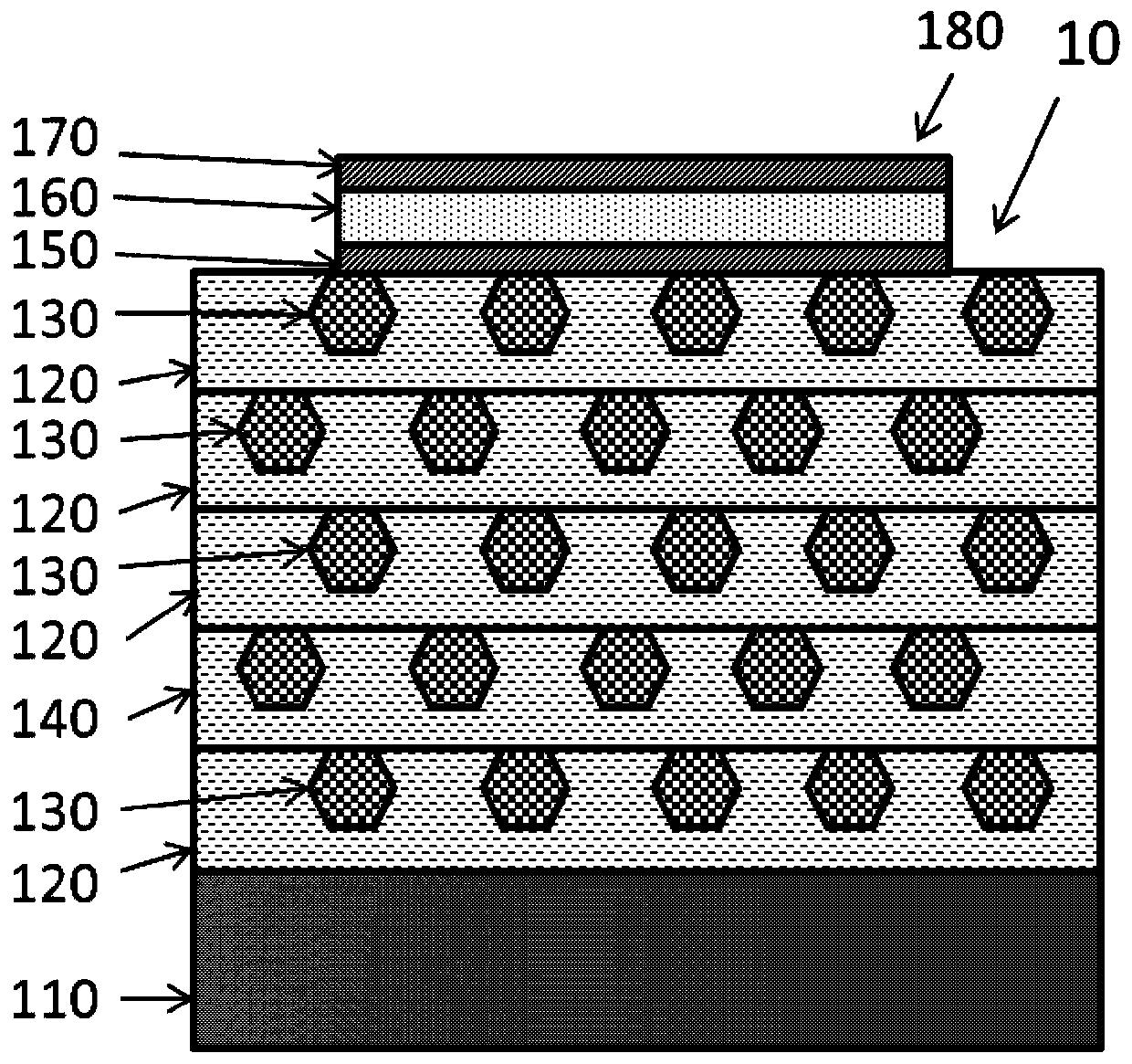
[0024] Such as figure 2 As shown, the thin-film bulk acoustic resonator 10 based on phononic crystals of the present invention includes a substrate 110, the substrate material is high-resistance silicon; it includes a phononic crystal layer 140 formed on the front side of the substrate, formed on the phononic crystal The piezoelectric oscillator stack structure 180 on the layer 140; wherein the phononic crystal layer includes multiple layers of phononic crystals arranged periodically, and each layer of phononic crystals is arranged alternately and periodically with scatterers and substrates of different materials, such as scatterers 130 The material can be silicon dioxide, air and other low-sonic materials, and the material of the substrate 120 can be high-sonic materials such as tungsten, high-resistance silicon, and aluminum nitride; the scatterer structure in the phononic crystal described in this embodiment is regular hexagonal In the present invention, the phononic cryst...
Embodiment 3
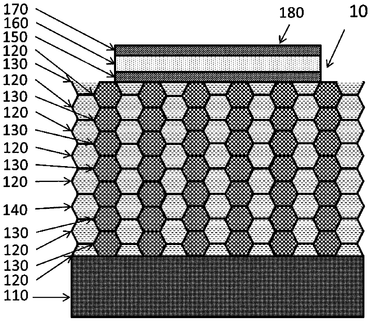
[0026] Such as Figure 3-4 As shown, the thin-film bulk acoustic resonator 10 based on phononic crystals of the present invention includes a substrate 110, the substrate material is high-resistance silicon; it includes a phononic crystal layer 140 formed on the front side of the substrate, formed on the phononic crystal The piezoelectric oscillator stack 180 on the layer 140; wherein the phononic crystal layer includes multiple layers of phononic crystals arranged periodically, and each layer of phononic crystals is arranged alternately and periodically with scatterers and substrates of different materials, such as the scatterer 130 material Low-sonic materials such as silicon dioxide and air can be selected, and high-sonic materials such as tungsten, high-resistance silicon, and aluminum nitride can be selected as the material of the substrate 120; the scatterer structure in the phononic crystal described in this embodiment is a regular hexagon Cylinder, the matrix structure ...
PUM
 Abstract
Description
Claims
Application Information
 - R&D
- Intellectual Property
- Life Sciences
- Materials
- Tech Scout
- Unparalleled Data Quality
- Higher Quality Content
- 60% Fewer Hallucinations
Browse by: Latest US Patents, China's latest patents, Technical Efficacy Thesaurus, Application Domain, Technology Topic, Popular Technical Reports.
© 2025 PatSnap. All rights reserved.Legal|Privacy policy|Modern Slavery Act Transparency Statement|Sitemap|About US| Contact US: help@patsnap.com


