3D bulk silicon microcapacitor based on MEMS technology, fabricating thereof and application

A capacitor, 3D technology, applied in capacitors, electrolytic capacitors, capacitor parts and other directions, can solve the problems of insufficient capacitance storage and specific energy density to meet demand, limited active material surface area and load quality, etc., to increase and decrease specific surface area. Comb width, the effect of stable physical and chemical properties

Active Publication Date: 2019-11-08
HUAZHONG UNIV OF SCI & TECH
View PDF6 Cites 6 Cited by
  • Summary
  • Abstract
  • Description
  • Claims
  • Application Information

AI Technical Summary

Problems solved by technology

The 3D comb tooth structure reported in the current literature, after the material is stacked and grown, has a thickness of several hundred nanometers to several microns, and the surface area and loading quality of the active material are limited, resulting in insufficient capacitance storage and specific energy density to meet the demand.

Method used


Image

  • 3D bulk silicon microcapacitor based on MEMS technology, fabricating thereof and application
  • 3D bulk silicon microcapacitor based on MEMS technology, fabricating thereof and application
  • 3D bulk silicon microcapacitor based on MEMS technology, fabricating thereof and application

Examples


Embodiment Construction

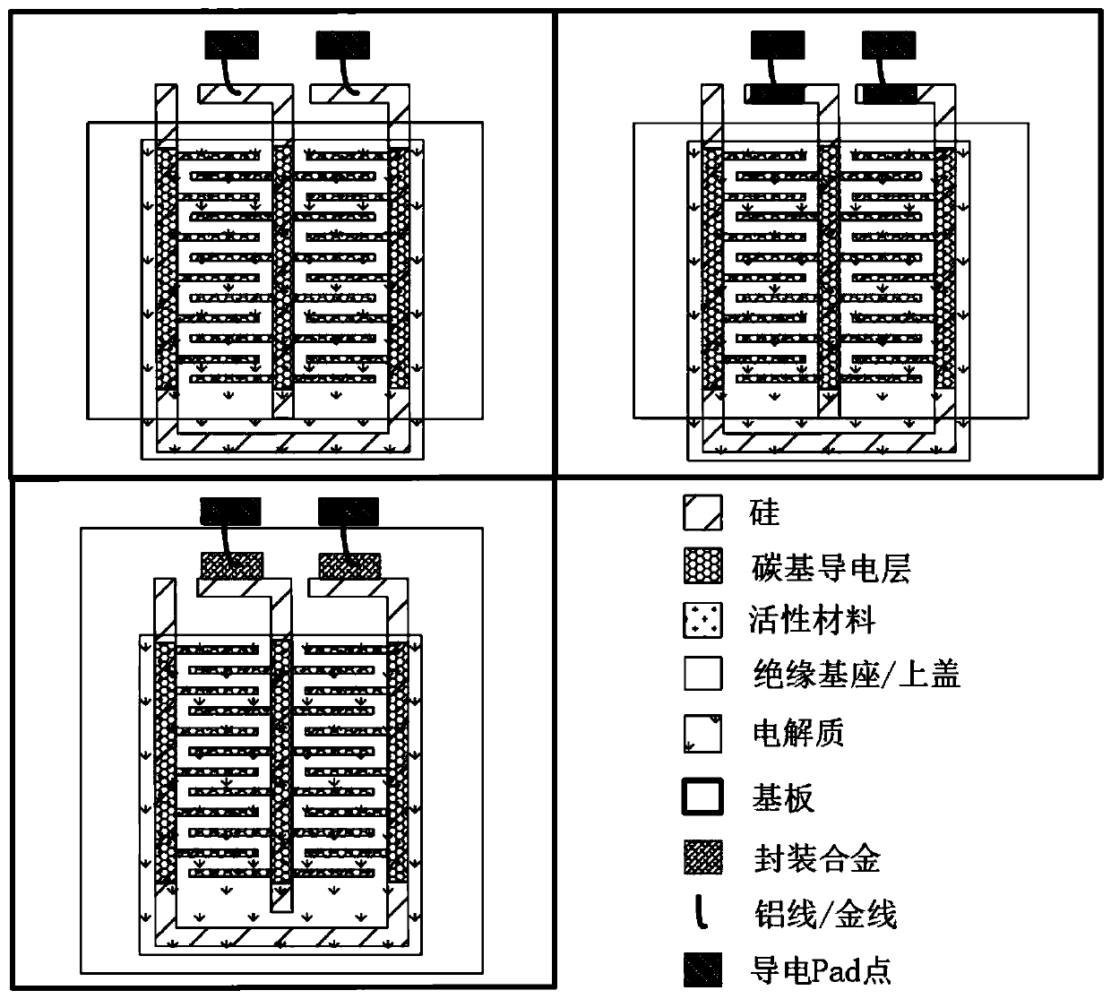
[0049] In order to make the object, technical solution and advantages of the present invention clearer, the present invention will be further described in detail below in conjunction with the accompanying drawings and embodiments. It should be understood that the specific embodiments described here are only used to explain the present invention, not to limit the present invention. In addition, the technical features involved in the various embodiments of the present invention described below can be combined with each other as long as they do not constitute a conflict with each other.

[0050] A kind of manufacturing method of 3D bulk silicon miniature capacitor provided by the present invention comprises the following steps:

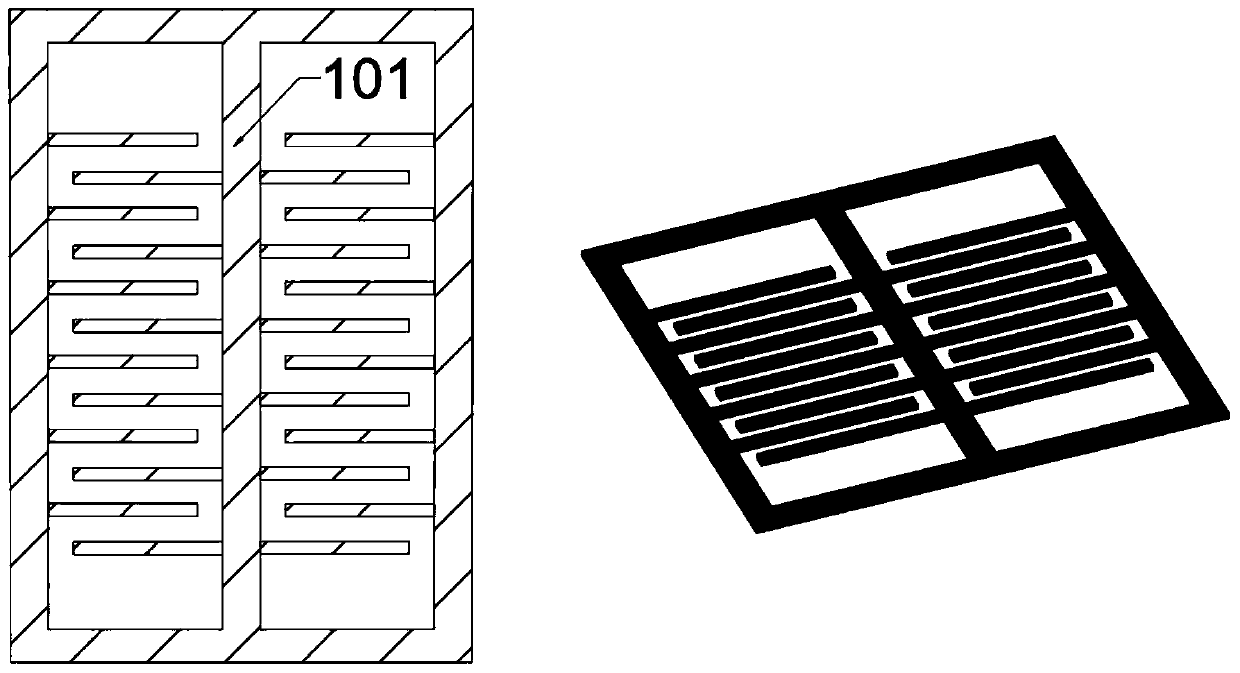
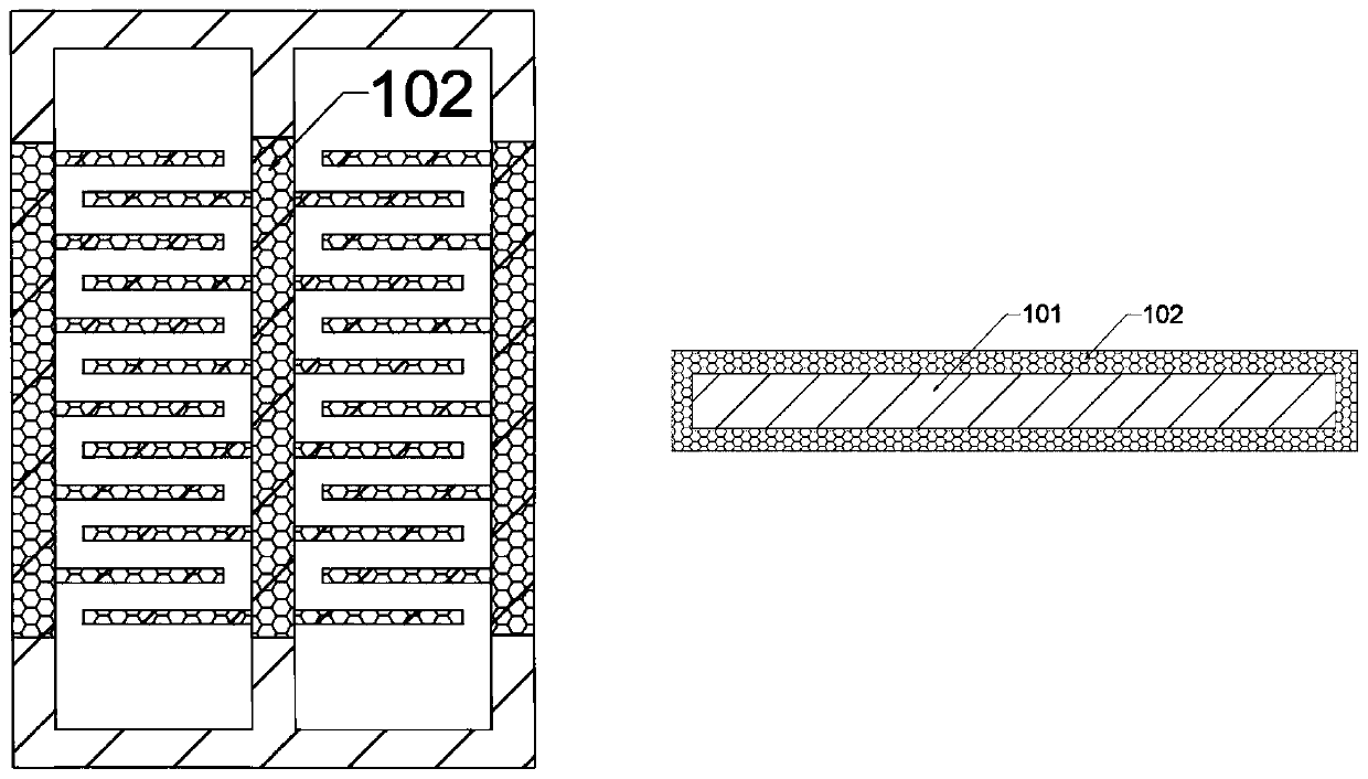
[0051] (1) Fabricate an array pattern on the surface of the silicon-based substrate by a photolithography process, perform etching according to the array pattern, and etch through the substrate to obtain a hollowed-out 3D bulk silicon electrode.

[0052...


PUM


Abstract

The invention discloses a method of fabricating a 3D bulk silicon microcapacitor, which comprises steps of fabricating of a 3D bulk silicon substrate structure, introduction of an active material forthe 3D structure and three kinds of packaging and integration of the capacitor. Firstly, deep silicon etching is carried out to obtain a hollow 3D silicon-based comb substrate; the upper surface, thelower surface and the side wall of the comb are then coated with a carbon-based conductive layer and the active material; and finally, a gel-like electrolyte is applied to the surface, packaging and integration are carried out, and the 3D bulk silicon microcapacitor is obtained. In comparison with the conventional comb planar structure, the longitudinal height of the microcapacitor electrode is extended, the available electrode surface area is expanded from a two-dimensional plane to a three-dimensional surface and longitudinal side wall, the 3D electrode can carry more active material, the specific capacitance and the specific energy density are thus enhanced, the 3D comb structure active material introduction method is of great significance for the research of 3D capacitors, and the proposed packaging and integration method ensures the stability and the service life of the capacitor.

Description

technical field [0001] The invention belongs to a manufacturing method of a micro energy storage device, in particular to the technical fields of micro-nano processing technology and nano-material preparation and application, more specifically, a 3D bulk silicon microcapacitor based on MEMS technology, its production and application. Background technique [0002] The rapid development of portable electronic devices has made miniaturized and easy-to-integrate power supplies a research hotspot. This energy storage device can not only increase the density of the device, realize the power supply function, but also integrate with the chip and simplify the overall structure of the system. Supercapacitors are attractive energy storage due to their high energy density, cycle efficiency, and charge-discharge ratio relative to batteries. Traditional supercapacitors are too bulky for tiny devices, and traditional fabrication methods are not compatible with microelectronics fabrication ...

Claims


Application Information

Patent Timeline
Patent Type & Authority Applications(China)
IPC IPC(8): H01G9/042H01G9/048H01G9/10H01G9/26B81C1/00
CPCB81C1/005B81C1/00523H01G9/042H01G9/048H01G9/10H01G9/26
Inventor 王玉容孙雷蒙肖东阳胡方靖涂良成
Owner HUAZHONG UNIV OF SCI & TECH
Why Eureka
Try Eureka