

LED vertical chip based on silicon substrate and preparation method thereof
A silicon substrate and chip technology, applied in the direction of electrical components, circuits, semiconductor devices, etc., can solve the problems of unstable yield rate, complex process, easy damage, etc., to reduce technical threshold and cost, avoid complex process, and improve current distribution effect
- Summary
- Abstract
- Description
- Claims
- Application Information
AI Technical Summary
Problems solved by technology
Method used
Image

Examples
preparation example Construction
[0057] A method for preparing an LED vertical chip based on a silicon substrate, comprising the following steps:
[0058] A. growing an epitaxial layer on a silicon substrate;
[0059] The epitaxial layer includes an N-type layer, a light-emitting layer and a P-type layer, and the size of the silicon substrate is 2-8 inches.
[0060] The epitaxial layer is grown on the silicon substrate by MOCVD process.
[0061]B. Prepare the current diffusion layer and the current blocking layer by photolithography on the epitaxial layer;
[0062] The material of the current diffusion layer includes one or more of indium tin oxide (ITO), fluorine tin oxide (FTO) and aluminum zinc oxide (AZO), with a thickness of 25-500nm.
[0063] Current blocking layer materials include silicon dioxide (SiO 2 ), silicon nitride (Si 3 N 4 ), titanium dioxide (TiO 2 ), with a thickness of 60-300nm.
[0064] C. prepare passivation layer and positive electrode further by photolithography;
[0065] The p...
Embodiment 1
[0080] A method for preparing an LED vertical chip based on a silicon substrate, comprising the following steps:
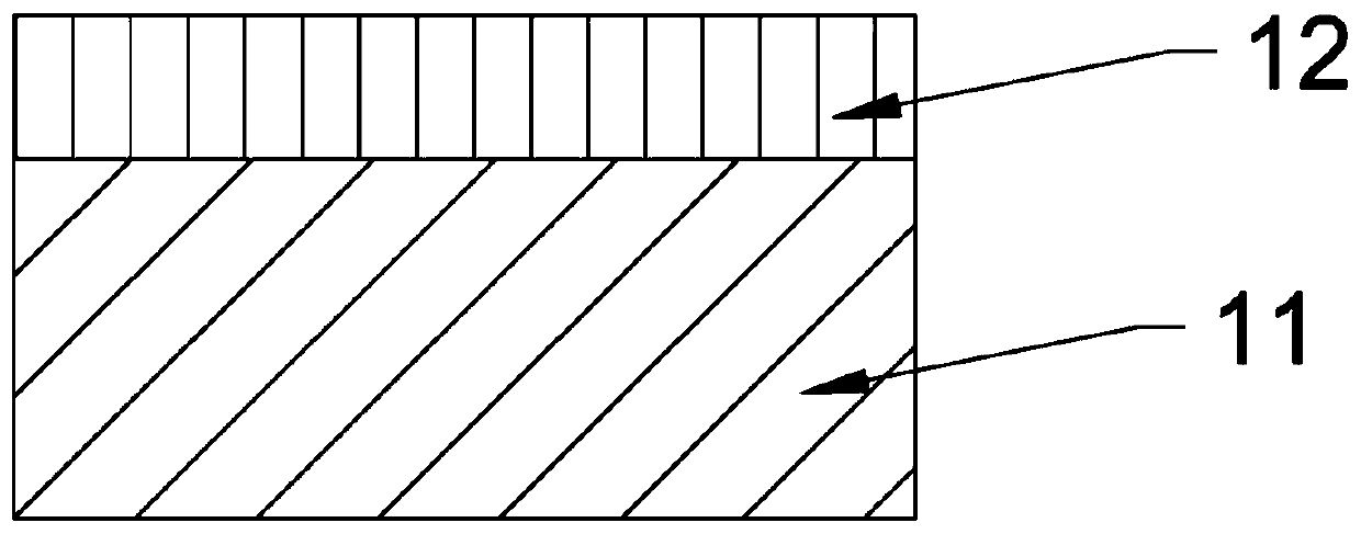
[0081] A. An epitaxial layer 12 is grown on a silicon substrate 11; the silicon substrate is a 4-inch silicon wafer, and the epitaxial layer 12 is composed of an N-type layer, a light-emitting layer, and a P-type layer, with a total thickness of 4.5 μm. The epitaxial layer 12 adopts MOCVD process grown on a silicon substrate 11, such as figure 1 shown;
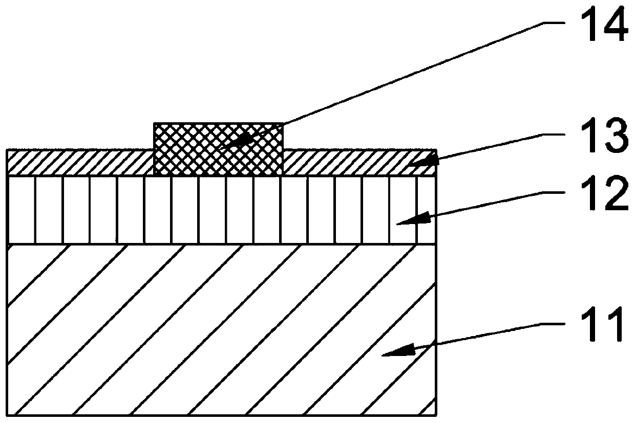
[0082] B. On the epitaxial layer 12, first deposit the current diffusion layer 13, preferably indium tin oxide (ITO), with a thickness of 80nm, and use photolithography to open the ITO, leaving the position of the current blocking layer 14; then deposit the current blocking layer 14 , preferably silicon dioxide (SiO 2 ), formed by PECVD plasma reaction deposition, with a thickness of 200nm, and using photolithography to pattern the current blocking layer 14, such as figure 2 shown;
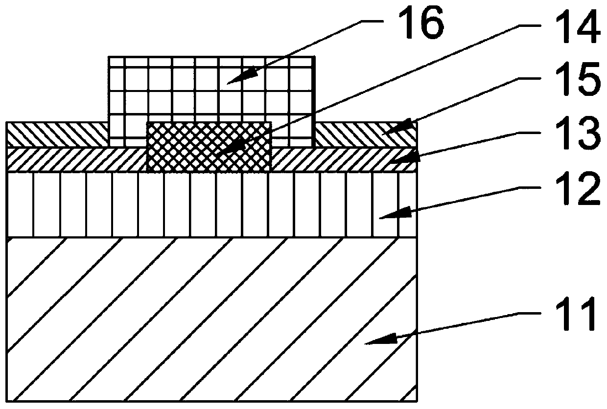
[0083] C. Further photoli...
Embodiment 2
[0090] A method for preparing an LED vertical chip based on a silicon substrate, comprising the following steps:
[0091] The preparation steps are the same as in Example 1, except that:
[0092] In step E, the silicon substrate 11 is photolithographically prepared to have different shapes of through holes, preferably square, and the periodic array is 3x3, such as Figure 10 shown.
PUM
| Property | Measurement | Unit |
|---|---|---|
| Thickness | aaaaa | aaaaa |
| Thickness | aaaaa | aaaaa |
| Thickness | aaaaa | aaaaa |
Abstract
Description
Claims
Application Information