Enhanced AlN/AlGaN/GaN HEMT device and preparation method thereof

An enhanced device technology, applied in semiconductor/solid-state device manufacturing, semiconductor devices, electrical components, etc., can solve problems such as difficulty in realizing enhanced devices, device failure, device damage, etc., and achieve threshold voltage and large saturation current enhancement mode device, high threshold voltage and high saturation current enhancement mode device, avoiding the effect of low saturation current density

Pending Publication Date: 2019-11-15
SOUTH CHINA UNIV OF TECH
View PDF0 Cites 5 Cited by
  • Summary
  • Abstract
  • Description
  • Claims
  • Application Information

AI Technical Summary

Problems solved by technology

Therefore, the p-type gate technology also has the problem that it is difficult to control the etching precision. Insufficient etching or excessive etching will reduce the concentration of two-dimensional electron gas under the channel and reduce the output current.
[0008] It can be seen that although the above methods can realize enhanced devices, they will cause damage to the device more or less, resulting in a decrease in output current density, an increase in gate leakage current, a decrease in device stability, and even device failure. This is also the main reason why it is difficult to realize high threshold voltage and large saturation current enhanced device

Method used


Image

  • Enhanced AlN/AlGaN/GaN HEMT device and preparation method thereof
  • Enhanced AlN/AlGaN/GaN HEMT device and preparation method thereof
  • Enhanced AlN/AlGaN/GaN HEMT device and preparation method thereof

Examples


Embodiment 1

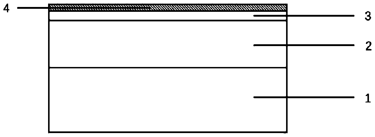
[0053] An enhanced AlN / AlGaN / GaN HEMT device in this embodiment, its structural schematic diagram is as follows figure 1 shown. Including: substrate 1, GaN channel layer 2, AlGaN ultra-thin barrier layer 3, amorphous SiO 2 Layer 4, single crystal AlN layer 5, drain metal electrode 6, source metal electrode 7 and gate metal electrode 8, wherein:

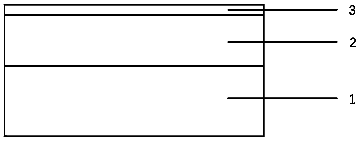
[0054] The substrate 1, GaN channel layer 2 and AlGaN ultra-thin barrier layer 3 are stacked sequentially from bottom to top;

[0055] The amorphous SiO 2 Layer 4 covers a part of the upper surface of the AlGaN ultra-thin barrier layer 3;

[0056] The drain metal electrode 6 and the source metal electrode 7 are located on the upper surface of the AlGaN ultra-thin barrier layer 3 and are not covered with amorphous SiO 2 On both sides covered by the layer 4, ohmic contact is formed between the drain metal electrode 6 and the source metal electrode 7 and the AlGaN ultra-thin barrier layer 3;

[0057] The single crystal AlN layer 5 c...

Embodiment 2

[0070] An enhanced AlN / AlGaN / GaN HEMT device in this embodiment, its structural schematic diagram is as follows figure 1 As shown, it includes: substrate 1, GaN channel layer 2, AlGaN ultra-thin barrier layer 3, amorphous SiO2 layer 4, single crystal AlN layer 5, drain metal electrode 6, source metal electrode 7 and gate metal electrode 8, in:

[0071] The substrate 1, GaN channel layer 2 and AlGaN ultra-thin barrier layer 3 are stacked sequentially from bottom to top;

[0072] The amorphous SiO 2 Layer 4 covers a part of the upper surface of the AlGaN ultra-thin barrier layer 3;

[0073] The drain metal electrode 6 and the source metal electrode 7 are located on the upper surface of the AlGaN ultra-thin barrier layer 3 and are not covered with amorphous SiO 2 On both sides covered by the layer 4, ohmic contact is formed between the drain metal electrode 6 and the source metal electrode 7 and the AlGaN ultra-thin barrier layer 3;

[0074] The single crystal AlN layer 5 cov...

Embodiment 3

[0087] An enhanced AlN / AlGaN / GaN HEMT device in this embodiment, its structural schematic diagram is as follows figure 1 As shown, it includes: substrate 1, GaN channel layer 2, AlGaN ultra-thin barrier layer 3, amorphous SiO2 layer 4, single crystal AlN layer 5, drain metal electrode 6, source metal electrode 7 and gate metal electrode 8, in:

[0088] The substrate 1, GaN channel layer 2 and AlGaN ultra-thin barrier layer 3 are stacked sequentially from bottom to top;

[0089] The amorphous SiO2 layer 4 covers a part of the upper surface of the AlGaN ultra-thin barrier layer 3;

[0090] The drain metal electrode 6 and the source metal electrode 7 are respectively located on the two sides of the upper surface of the AlGaN ultra-thin barrier layer 3 that are not covered by the amorphous SiO2 layer 4, and the drain metal electrode 6 and the source metal electrode 7 are connected to the AlGaN ultra-thin barrier layer. Ohmic contact is formed between layers 3;

[0091] The sing...


PUM

PropertyMeasurementUnit
thicknessaaaaaaaaaa
thicknessaaaaaaaaaa
thicknessaaaaaaaaaa

Abstract

The invention belongs to the field of semiconductor devices and discloses an enhanced AlN/AlGaN/GaN HEMT device and a preparation method thereof. The device includes a substrate, a GaN channel layer,an AlGaN ultra-thin barrier layer, an amorphous SiO2 layer, a single-crystal AlN layer, a drain metal electrode, a source metal electrode and a gate metal electrode. The enhanced device of the presentinvention is based on GaN and an ultra-thin AlGaN heterojunction, and the single-crystal AlN layer is epitaxially formed on the heterojunction after inserting an amorphous SiO2 layer in a region under a gate. The amorphous SiO2 layer under the gate can isolate the polarization enhancement effect of the highly polar single-crystal AlN layer on the AlGaN ultra-thin barrier layer, a two-dimensionalelectron gas under the gate is depleted, the device is turned off, and the enhanced device is realized. At the same time, the amorphous SiO2 under the gate and the single-crystal AlN can be used as adielectric layer under the gate, the reduction of the gate leakage current is facilitated, and the breakdown voltage of the device is increased.

Description

technical field [0001] The invention belongs to the field of semiconductor devices, and in particular relates to an enhanced AlN / AlGaN / GaN HEMT device and a preparation method thereof. Background technique [0002] Among compound semiconductor electronic devices, high electron mobility transistors (HEMTs) are the most important electronic devices used in high-frequency and high-power applications. This device relies on the spontaneous polarization and piezoelectric polarization effects of group III nitride semiconductors to form a two-dimensional electron gas (2DEG) conduction channel with quantum effects at the heterojunction interface. The density, mobility and saturation rate of 2DEG etc. determine the current handling capability of the device. Among them, HEMT devices based on GaN and related III-V nitride materials (AlN, InN) are currently the research hotspots of compound semiconductor electronic devices. Compared with the second-generation semiconductor GaAs, GaN ha...

Claims


Application Information

Patent Timeline
Patent Type & Authority Applications(China)
IPC IPC(8): H01L29/06H01L29/20H01L29/423H01L29/51H01L29/778H01L21/28H01L21/335
CPCH01L29/0611H01L29/0638H01L29/0649H01L29/2003H01L29/401H01L29/42364H01L29/51H01L29/513H01L29/517H01L29/66462H01L29/7787
Inventor 李国强孙佩椰陈丁波万利军阙显沣姚书南
Owner SOUTH CHINA UNIV OF TECH
Why Eureka
Try Eureka