Supercharge Your Innovation With Domain-Expert AI Agents!

Charging contact structure and preparation method thereof

A charging contact and electrolytic metal technology, which is applied to contact parts, electrical components, printed circuits, etc., can solve the problems that the coating cannot be charged, the coating is electrolyzed, and the static test of artificial sweat cannot pass the salt spray test, etc., so as to improve the flatness and smoothness, solve high temperature demagnetization, and facilitate SMT to the effect of printed circuit board

Inactive Publication Date: 2019-11-26
WWZN INFORMATION TECH CO LTD
View PDF5 Cites 3 Cited by
  • Summary
  • Abstract
  • Description
  • Claims
  • Application Information

AI Technical Summary

Problems solved by technology

However, the charging contact structure with Ni-Cu-Ni coating, Cu-Ni coating or Cu coating has the following problems: 1) the surface coating is easy to burst during SMT; 2) it cannot pass the salt spray test and artificial sweat static test; 3) If the artificial sweat electrolysis test is carried out after SMT, all the coatings will be electrolyzed within 1 minute, resulting in failure to charge
The charging contact structure with Ni-Cu-Ni-Au-Ag-Pd-Au plating layer can not pass the artificial sweat electrolysis test very well, for example, after charging after SMT, all the plating layers will be electrolyzed off within 1 minute causing can't charge

Method used


Image

  • Charging contact structure and preparation method thereof
  • Charging contact structure and preparation method thereof
  • Charging contact structure and preparation method thereof

Examples


preparation example Construction

[0051] In the second aspect, the embodiment of the present invention provides a method for preparing the charging contact structure described in the first aspect of the embodiment of the present invention, including: selecting the magnet substrate with specific specifications; performing electroplating on the surface of the magnet substrate, Forming a coating layer; performing hole sealing treatment on the surface of the coating layer to obtain a magnet base material with a coating layer; performing magnetization treatment on the magnet base material with a coating layer to obtain a charging contact structure.

[0052] In a further embodiment, the preparation method of the charging contact structure further includes: SMT the magnet substrate with the coating into the printed circuit board, and then perform magnetization treatment on the magnet substrate with the coating, Get the charging contact structure.

[0053] In this embodiment, the sealing treatment refers to sealing th...

Embodiment 1

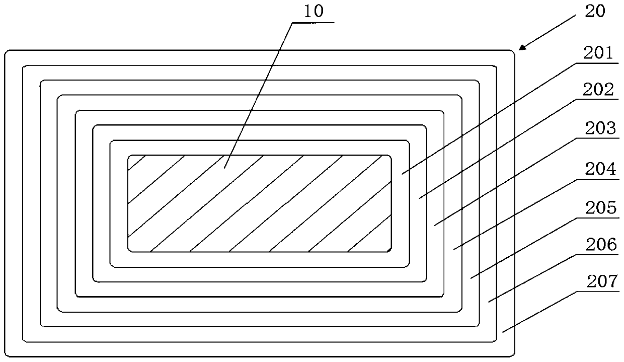
[0056] figure 1 It is a schematic diagram of the coating on NdFeB in Example 1 of the present invention. A charging contact structure, comprising: NdFeB 10, the surface of NdFeB 10 is covered with a coating 20; the coating 20 is in turn from the inside to the outside of a pyro copper coating 201, an acid copper layer 202, a CuSnZn coating 203, a Pd coating 204, The first Au plating layer 205 , the RhRu alloy plating layer 206 and the second Au plating layer 207 . The thickness of the burnt copper plating layer 201 is 8μ-10μ, the thickness of the acid copper layer 202 is 18μ-20μ, the thickness of the CuSnZn plating layer 203 is 2μ-4.5μ, the thickness of the Pd plating layer 204 is 0.6μ-0.75μ, the first Au plating layer 205 The thickness of the RhRu alloy plating layer 206 is 0.75μ-1μ, the thickness of the second Au plating layer 207 is 0.125μ-0.25μ, and the second Au plating layer 207 is the plating layer after sealing treatment.

[0057] A method for preparing a charging con...

Embodiment 2

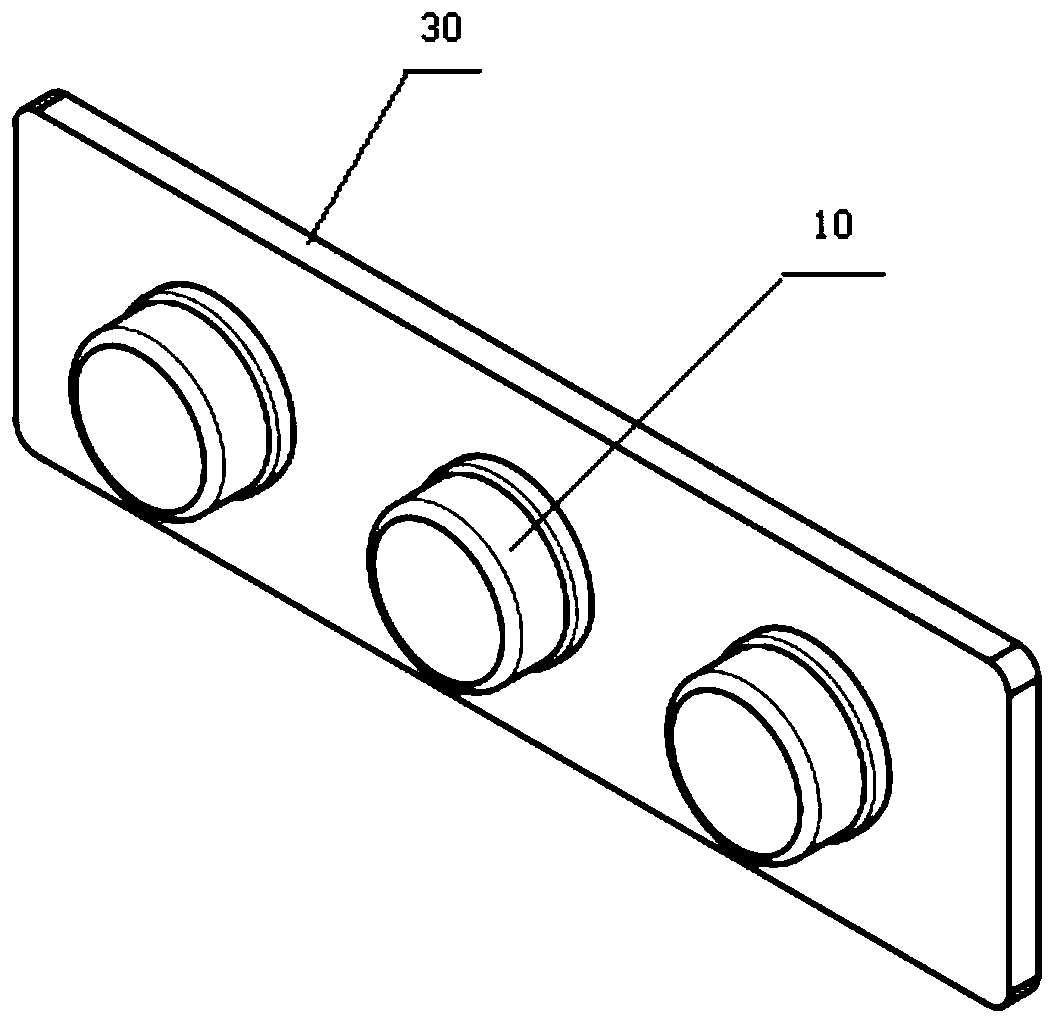
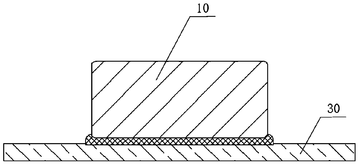
[0073] figure 2 It is a schematic diagram of the charging contact structure in Embodiment 2 of the present invention; image 3 It is a cross-sectional view of the charging contact structure in Embodiment 2 of the present invention. A charging contact structure, comprising: NdFeB 10 and a printed circuit board 30, the NdFeB 10 is connected to the printed circuit board 30 by surface mounting; the surface of the NdFeB 10 is covered with a coating 20; the coating 20 is from the inside to the The outer layers are pyro-copper coating 201 , acid copper coating 202 , CuSnZn coating 203 , Pd coating 204 , first Au coating 205 , RhRu alloy coating 206 and second Au coating 207 . The thickness of the burnt copper plating layer 201 is 8μ-10μ, the thickness of the acid copper layer 202 is 18μ-20μ, the thickness of the CuSnZn plating layer 203 is 2μ-4.5μ, the thickness of the Pd plating layer 204 is 0.6μ-0.75μ, the first Au plating layer 205 The thickness of the RhRu alloy plating layer ...


PUM


Abstract

The invention discloses a charging contact structure and a preparation method thereof. The charging contact structure comprises a magnet substrate and an anti-synthetic perspiration electrolytic metallayer; a surface of the magnet substrate is coated with a plating layer; the plating layer sequentially includes an anti-corrosive metal layer, an acid copper layer, a metal barrier layer from insideto outside. According to the embodiment disclosed by the invention, through electroplating of a special functional plating layer on the magnet substrate, not only the flatness and smoothness of the surface of the magnet substrate are improved, but also the effects that the magnet substrate has the performances of salt spray resistance testing, the anti-synthetic perspiration static testing and anti-synthetic perspiration electrolytic testing after an SMT (Surface Mounted Technology); and the problems that the magnet substrate in the existing charging contact structure cannot be subject to SMTor cannot be charged after being subject to SMT are solved. According to the embodiment disclosed by the invention, the magnet substrate with the coating layer is mounted to a printed circuit board through the SMT and is then magnetized; and the problems that the conventional magnets attract with each other after being magnetized and subjected to SMT and the magnets are demagnetized after encountering heat are solved.

Description

technical field [0001] The invention relates to the technical field of charging devices, in particular to a charging contact structure and a preparation method thereof. Background technique [0002] At present, the commonly used charging methods for smart wearable products include the connector method and the charging contact plus shrapnel or connector (Pogo pin) method; for example, Bluetooth wireless headsets and charging boxes use the Pogo pin charging method. Among them, the base material of the charging contact and the electroplating scheme often encounter two problems: first, the surface mount technology (SMT) soldering cannot be done after the traditional magnet electroplating; second, the contact on the product is subjected to At the same time, the friction force will also be electrolyzed by the current in the state of sweat, and the plating layer will fall off. After the plating layer falls off, the internal magnetic material that is easily oxidized is exposed, whic...

Claims


Application Information

Patent Timeline
Patent Type & Authority Applications(China)
IPC IPC(8): H01R13/03H05K1/18C25D5/14C25D5/12C25D5/10
CPCC25D5/10C25D5/12C25D5/14H01R13/03H05K1/181
Inventor 刘玉友曾森
Owner WWZN INFORMATION TECH CO LTD
Features
  • R&D
  • Intellectual Property
  • Life Sciences
  • Materials
  • Tech Scout
  • Unparalleled Data Quality
  • Higher Quality Content
  • 60% Fewer Hallucinations
Learn More