
A split-gate 4h-sic VDMOS device

A split gate and device technology, which is applied in semiconductor devices, electrical components, circuits, etc., can solve the problems of low reliability of body diodes, increase the complexity of circuit design, and cost, and achieve the effect of suppressing pinch-off, improving dynamic performance, Effect of Cgd reduction

Active Publication Date: 2021-06-04
HANGZHOU SILICON-MAGIC SEMICON TECH CO LTD
View PDF6 Cites 0 Cited by
  • Summary
  • Abstract
  • Description
  • Claims
  • Application Information

AI Technical Summary

Problems solved by technology

The reliability of the body diode of the MOSFET is low. In engineering, a diode is usually connected in series with the drain of the MOSFET to prevent the conduction of the parasitic body diode, and then an additional anti-parallel Schottky diode is connected at both ends of the drain and source to provide a new freewheeling path. Obviously , this method greatly increases the complexity and cost of circuit design

Method used


Image

  • A split-gate 4h-sic VDMOS device
  • A split-gate 4h-sic VDMOS device
  • A split-gate 4h-sic VDMOS device

Examples


Embodiment Construction

[0030] The principles and features of the present invention are described below in conjunction with the accompanying drawings, and the examples given are only used to explain the present invention, and are not intended to limit the scope of the present invention.

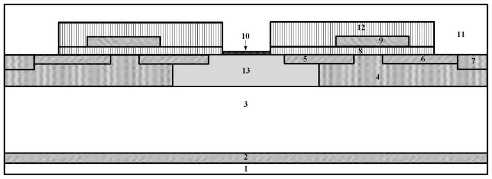
[0031] Such as figure 1 As shown, a split gate 4H-SiC VDMOS device provided by an embodiment of the present invention includes: a drain 1, an N+ substrate 2, an N- epitaxial layer 3, a P well 4, a first N+ region 5, and an N+ source region 6 , P+ contact region 7, gate oxide layer 8, gate 9, Schottky contact 10, source 11, SiO 2 interlayer dielectric 12 and JFET region 13;

[0032] The drain 1, the N+ substrate 2 and the N- epitaxial layer 3 are sequentially stacked from bottom to top;

[0033] The JFET region 13 is located on the upper layer of the N- epitaxial layer 3;

[0034] The P well 4 is located on the upper layer of the N- epitaxial layer 3 and on both sides of the JFET region 13, the first N+ region 5 i...


PUM


Abstract

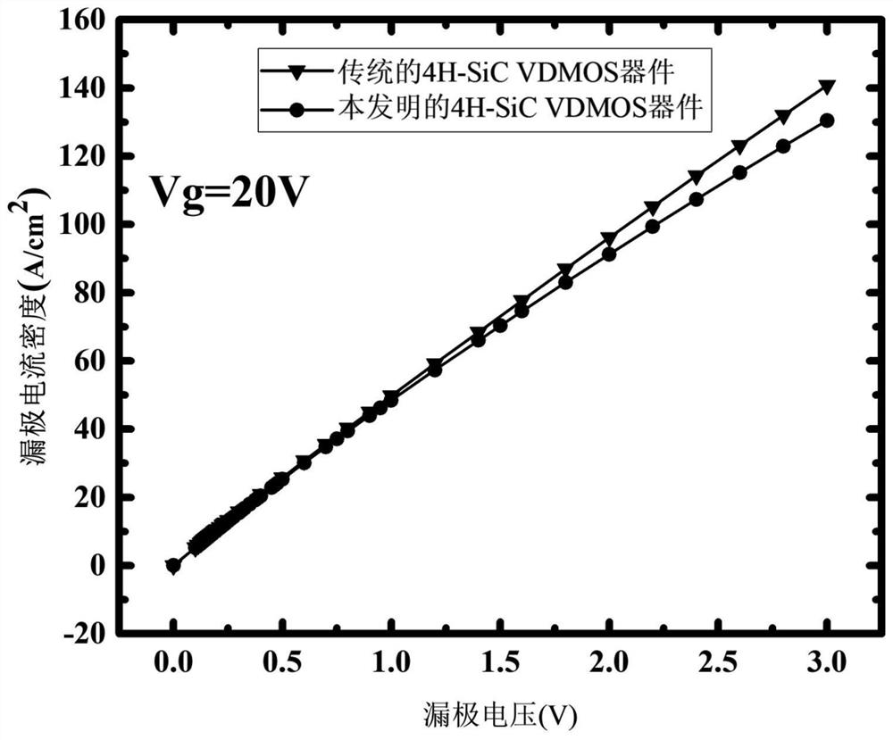
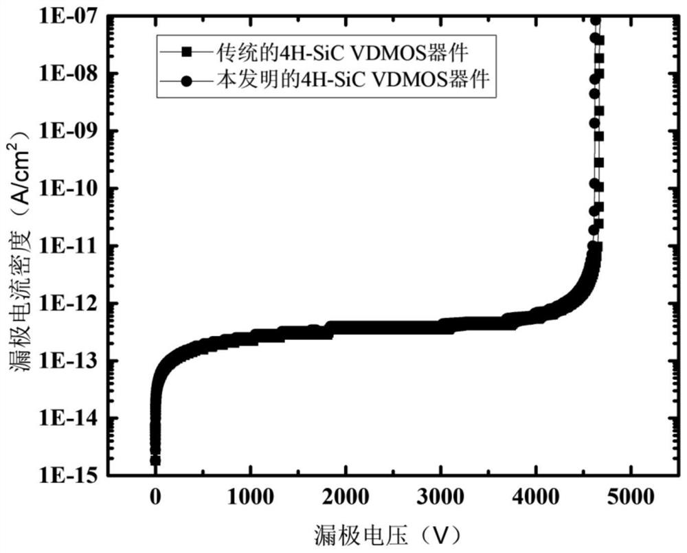
The invention relates to a split gate 4H-SiC VDMOS device, belonging to the technical field of power semiconductors. The device of the present invention adopts a split gate structure, integrates a Schottky diode in the middle of the split gate, and adds a first N+ region for adjusting forward characteristics. The Schottky contact located above the JFET region provides a current path during the reverse recovery process, which can reduce the reverse storage charge of the body diode and speed up the reverse recovery process; the increased first N+ region provides A conductive channel is created, which reduces the on-resistance of the device, making it consistent with conventional devices. The 4H-SiC VDMOS structure of the present invention has better switching characteristics and reverse recovery performance, and can ensure that the static characteristics are basically consistent with the traditional structure.

Description

technical field [0001] The invention belongs to the technical field of power semiconductors, in particular to a split gate 4H-SiC VDMOS device. Background technique [0002] SiC material is a typical representative of the third-generation wide-bandgap semiconductor material. Due to its advantages such as high critical breakdown electric field strength, high carrier saturation drift velocity, and high thermal conductivity, it has become a high-power , high temperature, high frequency, ideal material for radiation resistant devices. [0003] After more than 20 years of rapid development, SiC power devices have achieved impressive results. For example, 600V, 1200V, 1700V, 3300V, and 10kV SiC MOSFET devices have been successfully developed, and 600V, 1200V, and 1700V SiC MOSFET devices have been commercialized. But there is still a lot of room for improvement in power devices made of SiC materials. Taking SiC MOSFET as an example, the gate-to-drain capacitance Cgd of MOSFET af...

Claims


Application Information

Patent Timeline
Patent Type & Authority Patents(China)
IPC IPC(8): H01L29/78H01L29/47H01L29/423H01L29/10
CPCH01L29/1095H01L29/42376H01L29/47H01L29/7802H01L29/7803
Inventor 张有润钟炜王帅杨啸杨锐罗佳敏张波
Owner HANGZHOU SILICON-MAGIC SEMICON TECH CO LTD
Learn More