Method for in-situ study of amorphization mechanism of germanium-antimony-tellurium material under electron beam irradiation
A technology of electron beam irradiation and amorphization, which is applied in the field of research on the structure evolution of phase change materials, can solve the problems of inability to reflect the structure of materials, difficulty in in-situ observation, and confusion about the mechanism of amorphization, and achieve convenient research methods, The effect of sound experimental evidence
- Summary
- Abstract
- Description
- Claims
- Application Information
AI Technical Summary
Problems solved by technology
Method used
Image
Examples
Embodiment 1
[0055] This implementation takes the study of the amorphization process of germanium, antimony and tellurium materials from cubic phase to amorphous phase as an example. The specific process is as follows:
[0056] Step 1: Select a germanium, antimony and tellurium cubic phase crystal thin film deposited on a standard-sized carbon-supported copper mesh for transmission electron microscopy. The diameter of the carbon-supported copper mesh is 3 mm, and the final thickness of the film is 90 nm.
[0057] Step 2: Use plasma cleaning technology to pretreat the surface of the prepared film samples. In order to avoid oxidation, argon gas should be selected for plasma cleaning, and the cleaning time is set to 3 minutes;
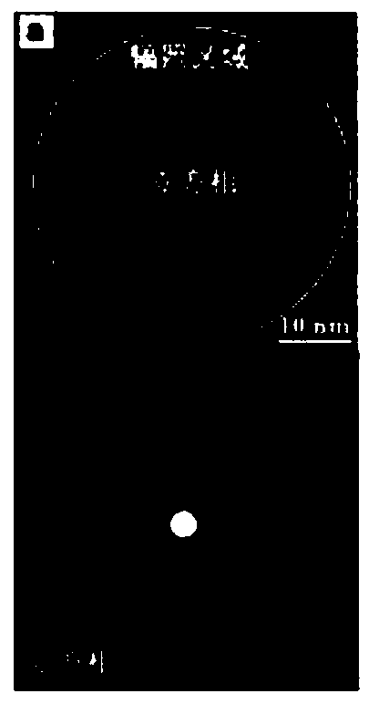
[0058] Step 3: Place the pretreated electron microscope sample in a transmission electron microscope, and look for an area with flat surface, no carbon deposition, no pollution, no damage and uniform thickness in the thin film sample as the irradiation area, such as f...
Embodiment 2
[0062] This implementation takes the study of the metastability and amorphization process of germanium, antimony and tellurium materials from hexagonal phase to amorphous phase as an example. The specific process is as follows:
[0063] Step 1: Select a germanium antimony tellurium hexagonal phase crystal thin film deposited on a standard size carbon support film copper grid for transmission electron microscopy, and the final thickness of the thin film is 80 nm.
[0064] Step 2: Use plasma cleaning technology to pretreat the surface of the prepared film samples. In order to avoid oxidation, argon gas should be selected for plasma cleaning, and the cleaning time is set to 3 minutes;
[0065] Step 3: Place the pretreated electron microscope sample in a transmission electron microscope, and look for an area with flat surface, no carbon deposition, no pollution, no damage and uniform thickness in the thin film sample as the irradiation area, such as Figure 5 shown;
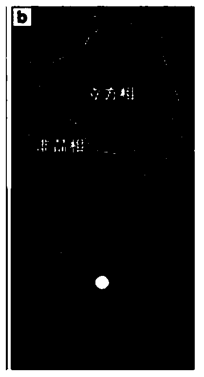
[0066] Step...
Embodiment 3
[0069] This implementation takes the study of the amorphization process of germanium, antimony and tellurium materials from cubic phase to amorphous phase as an example. The specific process is as follows:
[0070] Step 1: Select the germanium antimony tellurium cubic phase crystal thin film deposited on the carbon support film copper carrier grid of standard size for transmission electron microscope, and the final thickness of the thin film is 75nm.
[0071] Step 2: Use plasma cleaning technology to pretreat the surface of the prepared film samples. In order to avoid oxidation, argon gas should be selected for plasma cleaning, and the cleaning time is set to 3 minutes;
[0072] Step 3: Place the pretreated electron microscope sample in a transmission electron microscope, and look for an area with flat surface, no carbon deposition, no pollution, no damage and uniform thickness in the thin film sample as the irradiation area;
[0073] Step 4: Set the irradiation parameters and...
PUM
| Property | Measurement | Unit |
|---|---|---|
| diameter | aaaaa | aaaaa |
| thickness | aaaaa | aaaaa |
Abstract
Description
Claims
Application Information


