
Charging device and charging method for growing SiC single crystals by PVT (physical vapor transport) method

A charging device and single crystal technology, applied in the direction of single crystal growth, crystal growth, single crystal growth, etc., can solve the problems of blocking the upward transport of SiC gas phase components, unscientific charging methods, and reduced growth rate, etc., to achieve Reduce wrapping, strong caulking ability, and reduce carbonization of raw materials

Inactive Publication Date: 2019-12-13
HEBEI SYNLIGHT CRYSTAL CO LTD
View PDF3 Cites 3 Cited by
  • Summary
  • Abstract
  • Description
  • Claims
  • Application Information

AI Technical Summary

Problems solved by technology

However, there will be SiC crystal crystallization at the porous graphite network in the growth chamber, which blocks the upward transport of SiC gas phase components in the powder, greatly reduces the growth rate, and affects the yield.
[0005] A large part of the reason for the formation of C inclusions is that the charging method is unscientific, and the method of loading raw materials with different particle sizes into the crucible is unreasonable, so it is very necessary to optimize the charging method to reduce the formation of inclusions in the crystal

Method used


Image

  • Charging device and charging method for growing SiC single crystals by PVT (physical vapor transport) method

Examples


Embodiment 1

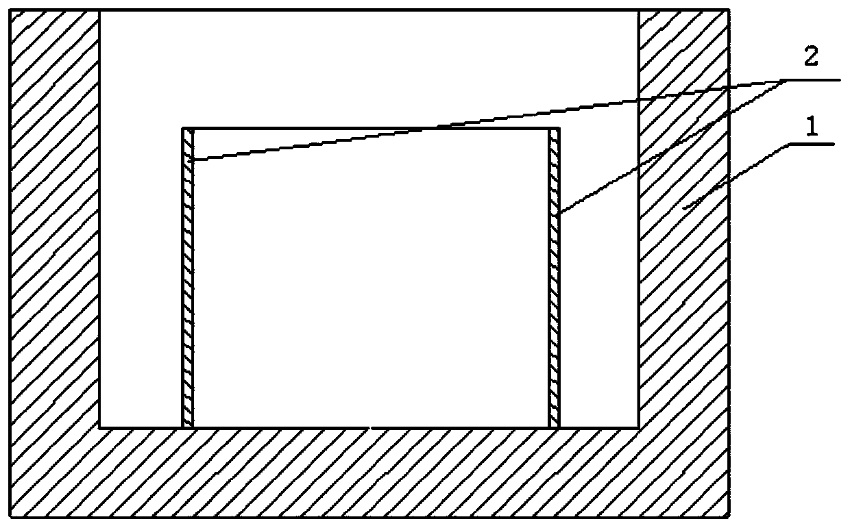
[0027] This embodiment provides a charging device for PVT growth of SiC single crystal, including a crucible 1 and an auxiliary charging device 2. The auxiliary charging device 2 is used to divide the side and middle of the inner space of the crucible 1 The auxiliary charging device 2 is cylindrical, the ratio of the cross-sectional area of ​​the auxiliary charging device 2 to the cross-sectional area of ​​the crucible is 4 / 9, and the auxiliary charging device 2 is made of graphite.

[0028] The charging method of this embodiment is as follows:

[0029] (1) Put an auxiliary charging device in the crucible to separate the side and middle of the inner space of the crucible;

[0030] (2) Select large-particle SiC raw materials and put them into the space inside the crucible;

[0031] (3) Select medium-sized SiC raw materials and load them into the lower layer of the middle space in the crucible;

[0032] (4) Select small particles of SiC raw material and put it into the upper layer of the...


PUM


Abstract

The invention discloses a charging device and charging method for growing SiC single crystals by a PVT (physical vapor transport) method, and belongs to the field of crystal growth. The device comprises a crucible and an auxiliary charging device for separating the side part and the middle part of the internal space of the crucible. According to the charging method, raw materials with different particle sizes are placed in different positions in the crucible; different functions are achieved; large-particle raw materials are located on the edge, thus the heat conductivity of a raw material area on the inner side of the crucible can be increased, and raw material carbonization generated by local overheating of the edge is reduced; and small-particle materials are located on the surface, thejoint filling capacity is high, and bottom carbonized C particles can be effectively prevented from being conveyed upwards. By adopting the charging method, inclusions in the crystals can be effectively reduced, the crystal quality can be improved, the crystals can be enabled to grow thicker, the yield can be increased, and meanwhile, no new material or new device is introduced, and the production cost is not additionally increased.

Description

Technical field [0001] The invention relates to the field of crystal growth, in particular to a charging device and a charging method for growing SiC single crystals by a PVT method. Background technique [0002] As a third-generation semiconductor material, SiC has many excellent properties such as wide band gap, high thermal conductivity, high electron saturation migration rate, and high breakdown electric field. Silicon carbide semiconductor has become an internationally recognized leader in power electronics, especially large The best electronic materials for the next 50 years of power power electronics can be used to make a new generation of high-efficiency and energy-saving power electronic devices, which are widely used in various fields of the national economy. [0003] In terms of SiC single crystal growth technology, the physical vapor transport (PVT) method is mainly used in the world to grow SiC single crystals. However, in the process of growing SiC single crystal by ...

Claims


Application Information

Patent Timeline
IPC IPC(8): C30B29/36C30B23/00
CPCC30B23/00C30B29/36
Inventor 刘新辉杨昆张福生路亚娟牛晓龙郑清超
Owner HEBEI SYNLIGHT CRYSTAL CO LTD
Learn More