Silicon carbide junction barrier Schottky diode with trench structure

A junction barrier Schottky, silicon carbide technology, applied in electrical components, circuits, semiconductor devices, etc., can solve the problems of reduced breakdown voltage of devices, deterioration of reverse breakdown characteristics, etc., to reduce electric field spikes , the effect of increasing forward conduction current and increasing width

Active Publication Date: 2019-12-13
UNIV OF ELECTRONICS SCI & TECH OF CHINA
View PDF8 Cites 10 Cited by
  • Summary
  • Abstract
  • Description
  • Claims
  • Application Information

AI Technical Summary

Problems solved by technology

However, increasing the width of the Schottky contact area will reduce the breakdown voltage of the device and deteriorate the reverse breakdown characteristics.

Method used


Image

  • Silicon carbide junction barrier Schottky diode with trench structure
  • Silicon carbide junction barrier Schottky diode with trench structure
  • Silicon carbide junction barrier Schottky diode with trench structure

Examples


Embodiment Construction

[0035] The principles and features of the present invention are described below in conjunction with the accompanying drawings, and the examples given are only used to explain the present invention, and are not intended to limit the scope of the present invention.

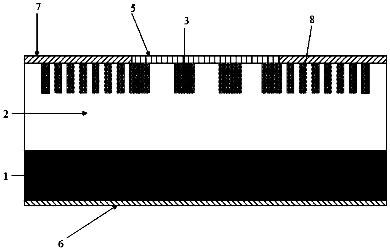
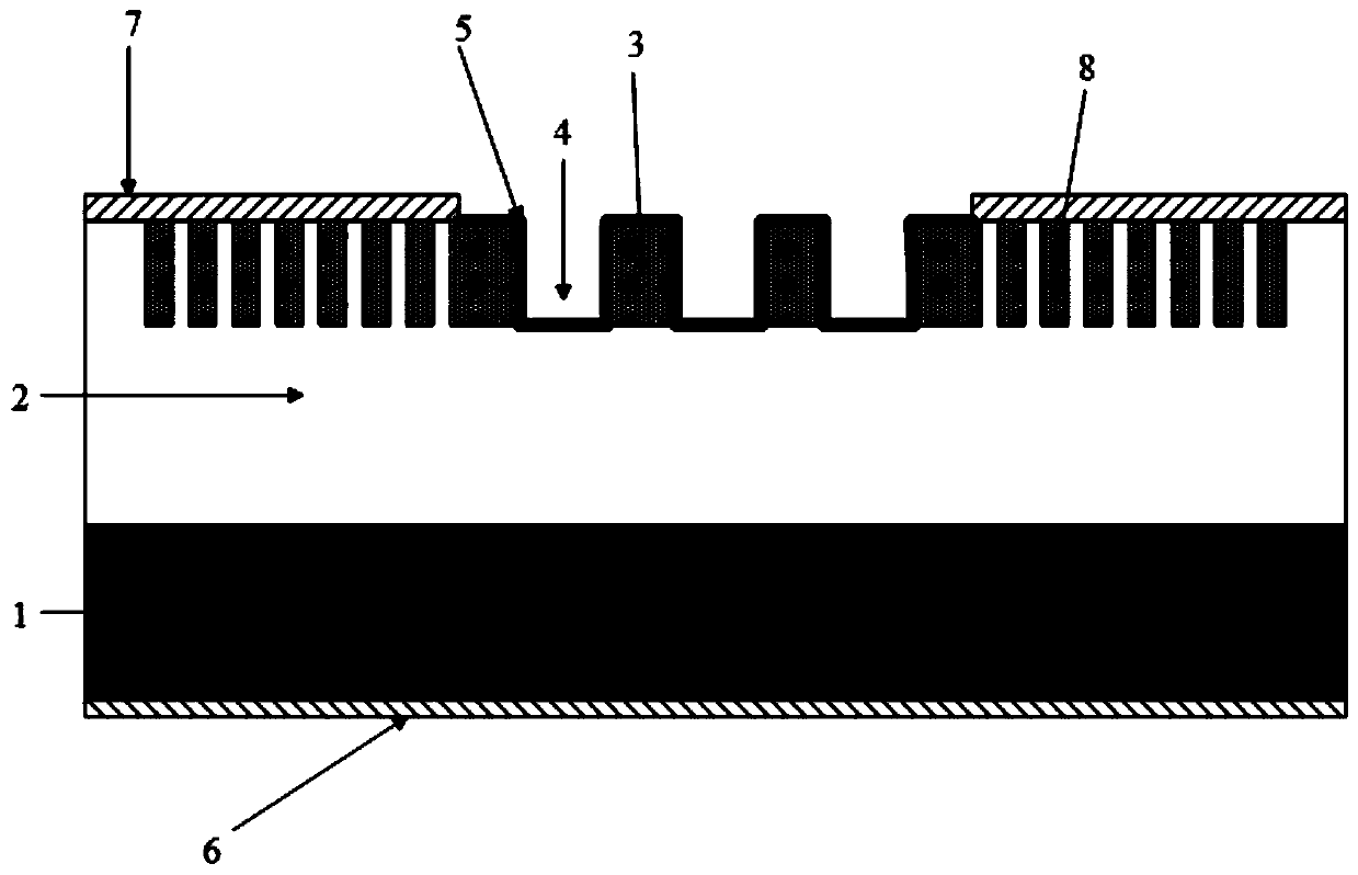
[0036] Such as figure 2 As shown, a silicon carbide junction barrier Schottky diode with a trench structure provided by the first embodiment of the present invention includes an ohmic contact electrode 6, a silicon carbide N+ substrate 1, a silicon carbide N- epitaxial layer 2, and SiO2 Isolation dielectric 7, Schottky contact electrode 5, multiple P+ injection regions 3 and multiple P+ field limiting rings 8;

[0037] Ohmic contact electrode 6, silicon carbide N+ substrate 1 and silicon carbide N- epitaxial layer 2 are sequentially stacked from bottom to top; multiple P+ implantation regions 3 are arranged at intervals on the upper layer of silicon carbide N- epitaxial layer 2; multiple P+ fields The confinement ...


PUM


Abstract

The invention relates to a silicon carbide junction barrier Schottky diode with a trench structure, and belongs to the technical field of semiconductor devices. According to the device, a Schottky contact region lower trench structure is introduced on the basis of the traditional JBS device structure, the size of a main junction edge peak electric field in the JBS region is reduced, the distribution of a main junction edge electric field during device breakdown is smoothened, the reverse withstand voltage of the device is improved, the forward conduction current of the device is also improved.Meanwhile, the structure can achieve a breakdown voltage value greater than that of the traditional SiC JBS device when the current is high and the Schottky contact region of the device is very wide,the reverse leakage current change is not obvious, and the problems such that the JBS device is poor in reverse breakdown voltage characteristic when the current is high and the Schottky contact region is very wide are solved.

Description

technical field [0001] The invention belongs to the technical field of semiconductor devices, and in particular relates to a silicon carbide junction barrier Schottky diode with a groove structure. Background technique [0002] Wide bandgap semiconductor material—silicon carbide (SiC) is an ideal material for preparing high-voltage power electronic devices. Compared with Si materials, SiC materials have a higher breakdown electric field strength (4×10 6 V / cm), high carrier saturation drift velocity (2×10 7 cm / s), high thermal conductivity, and good thermal stability, so it is especially suitable for high-power, high-pressure, high-temperature and radiation-resistant electronic devices. [0003] 4H-SiC Schottky barrier diode (SBD) is the first wide-bandgap power semiconductor device to replace silicon-based devices. Through the barrier formed by SiC semiconductor and metal contact, it realizes conduction in one direction and resistance in one direction. broken rectification...

Claims


Application Information

Patent Timeline
Patent Type & Authority Applications(China)
IPC IPC(8): H01L29/06H01L29/16H01L29/872
CPCH01L29/0615H01L29/0684H01L29/1608H01L29/872
Inventor 张有润罗茂久王帅陆超孟繁新贺晓金张波
Owner UNIV OF ELECTRONICS SCI & TECH OF CHINA
Why Eureka
Try Eureka