
Cr-Sb phase change storage material and preparation and application thereof
A phase-change storage, cr-sb technology, applied in the field of microelectronics, can solve problems such as difficulty in amorphization, and achieve the effects of fast crystallization, simple components, and reduced preparation process requirements.
- Summary
- Abstract
- Description
- Claims
- Application Information
AI Technical Summary
Problems solved by technology
Method used
Image

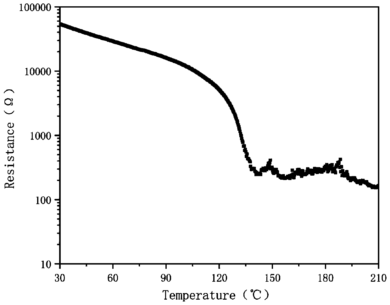
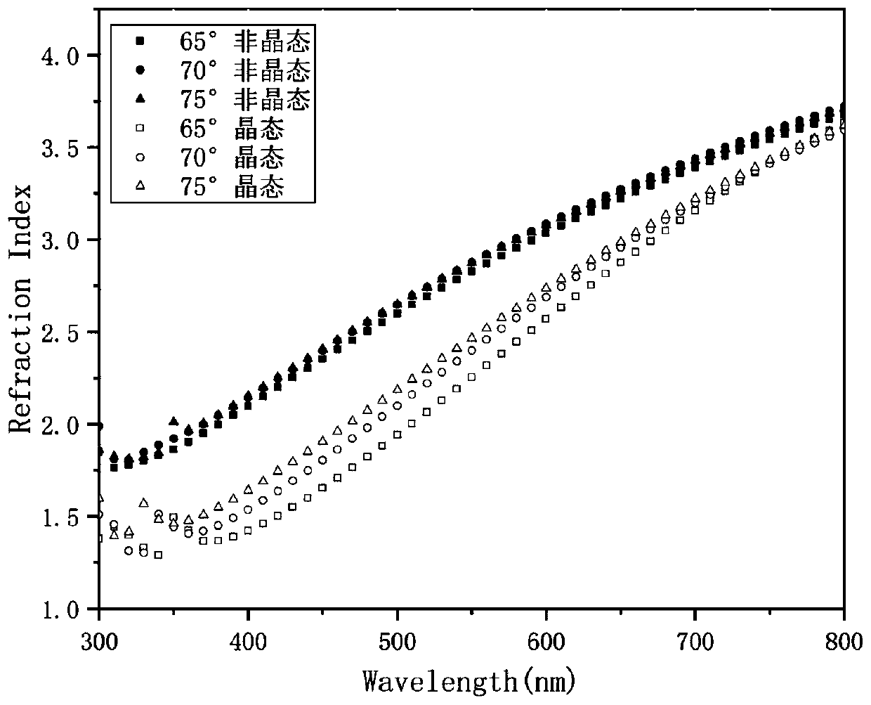
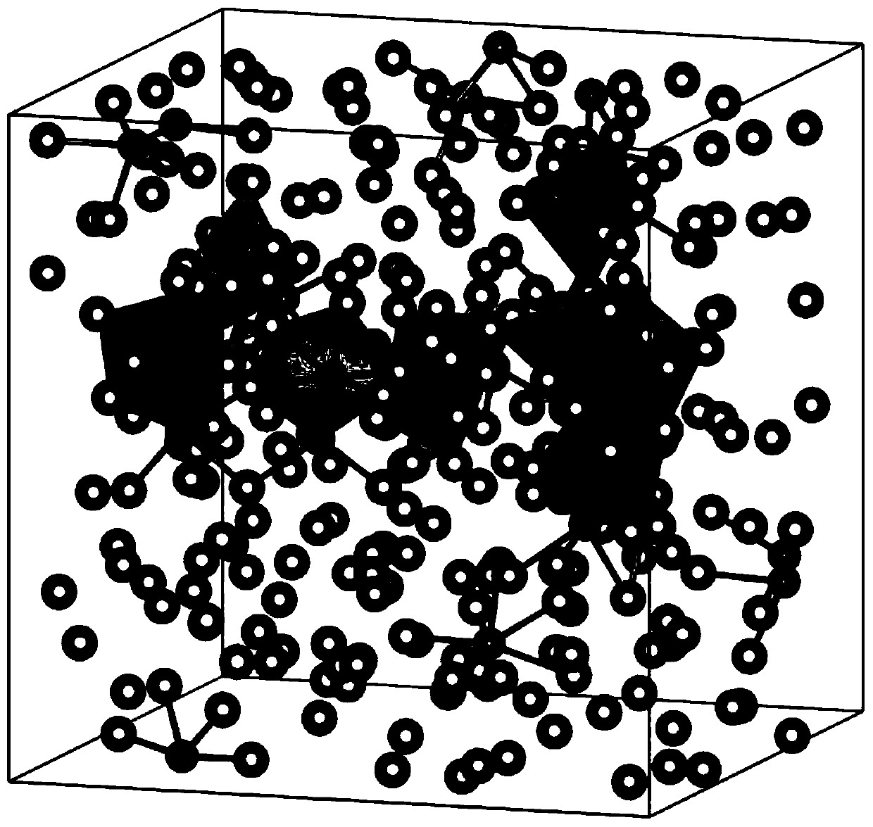
Examples
Embodiment 1
[0035] The general formula of the chemical composition of the nano-Cr-Sb phase-change film material used for phase-change memory prepared in this embodiment is Cr 10 Sb 90 .
[0036] The Cr-Sb nano film material is prepared by magnetron sputtering; during the preparation, high-purity argon is introduced as the sputtering gas, the sputtering pressure is 0.5 Pa, and the background vacuum is required to be 10 -4 Below Pa; the sputtering target is Cr 10 Sb 90 The alloy target is sputtered by a DC source, the sputtering power is 32W, and the target base distance is set to 120mm. Concrete preparation method comprises the following steps:
[0037] (1) Select SiO with a size of 1cm*1cm 2 / Si(100) substrate, clean the surface and back, remove dust particles, organic and inorganic impurities. Specifically, the following steps may be included:
[0038] (1-1) Cut out 1cm*1cm of SiO with a silicon wafer knife 2 / Si (100) substrate, used as the substrate for sputtering;
[0039] (1...
Embodiment 2
[0054] The general formula of the chemical composition of the nano-Cr-Sb phase-change film material used for phase-change memory prepared in this embodiment is Cr 5 Sb 95 .
[0055]The Cr-Sb nano film material is prepared by magnetron sputtering; during the preparation, high-purity argon is introduced as the sputtering gas, the sputtering pressure is 0.5 Pa, and the background vacuum is required to be 10 -4 Below Pa; the sputtering target is Cr 5 Sb 95 The alloy target is sputtered by a DC source, the sputtering power is 32W, and the target base distance is set to 120mm. Concrete preparation method comprises the following steps:
[0056] (1) Select SiO with a size of 1cm*1cm 2 / Si(100) substrate, clean the surface and back, remove dust particles, organic and inorganic impurities. Specifically, the following steps may be included:
[0057] (1-1) Cut out 1cm*1cm of SiO with a silicon wafer knife 2 / Si (100) substrate, used as the substrate for sputtering;
[0058] (1-2)...
Embodiment 3
[0070] The general formula of the chemical composition of the nano-Cr-Sb phase-change film material used for phase-change memory prepared in this embodiment is Cr 30 Sb 70 .
[0071] The Cr-Sb nano film material is prepared by magnetron sputtering; during the preparation, high-purity argon is introduced as the sputtering gas, the sputtering pressure is 0.5 Pa, and the background vacuum is required to be 10 -4 Below Pa; the sputtering target is Cr 30 Sb 70 The alloy target is sputtered by a DC source, the sputtering power is 32W, and the target base distance is set to 120mm. Concrete preparation method comprises the following steps:
[0072] (1) Select SiO with a size of 1cm*1cm 2 / Si(100) substrate, clean the surface and back, remove dust particles, organic and inorganic impurities. Specifically, the following steps may be included:
[0073] (1-1) Cut out 1cm*1cm of SiO with a silicon wafer knife 2 / Si (100) substrate, used as the substrate for sputtering;
[0074] (1...
PUM
 Abstract
Description
Claims
Application Information