Ultrathin solar black silicon wave absorber and preparation method thereof

A technology of sunlight and wave absorbers, applied in the field of silicon materials, can solve the problems of high manufacturing cost, complex structure design, and narrow operating frequency band of electromagnetic wave absorbers, and achieve the effect of low cost, simple structure, and enhanced coupling absorption

Active Publication Date: 2019-12-31
JIANGXI NORMAL UNIV
View PDF7 Cites 1 Cited by
  • Summary
  • Abstract
  • Description
  • Claims
  • Application Information

AI Technical Summary

Problems solved by technology

[0006] In order to solve the problems of narrow operating frequency band, complex structure design and high manufacturing cost of electromagnetic wave absorber, the present invention provides an ultra-thin solar black silicon absorber and its preparation method

Method used


Image

  • Ultrathin solar black silicon wave absorber and preparation method thereof
  • Ultrathin solar black silicon wave absorber and preparation method thereof
  • Ultrathin solar black silicon wave absorber and preparation method thereof

Examples


Embodiment Construction

[0029] The present invention will be further described below in conjunction with the accompanying drawings and specific embodiments.

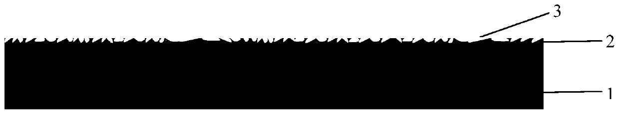
[0030] The ultra-thin solar black silicon absorber of the present invention can be prepared according to the following steps:

[0031] Step 1. Prepare silicon wafers, ultrasonically clean them with absolute ethanol, acetone, and deionized water in sequence, and then dry them to obtain pure silicon wafers;

[0032] Step 2, coating a layer of gold nano film on the surface of the pure silicon wafer by magnetron sputtering technology to obtain SI-Au samples;

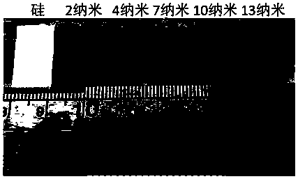
[0033] Step 3. Put the SI-Au sample into the muffle furnace, and perform constant temperature and timing heat treatment. The metal film becomes the metal particle layer, and the SI-AuNPs sample is obtained. The metal particles in the metal particle layer are of different sizes and have a radius of 50 nanometers to 200 nanometers;

[0034] Step 4, immerse the SI-AuNPs sample in a new etching...


PUM


Abstract

The invention provides an ultrathin solar black silicon wave absorber and a preparation method thereof. The ultrathin solar black silicon wave absorber includes a base layer and a metasurface structure layer. The metasurface structure layer is connected to the upper surface of the base layer. The base layer and the metasurface structure layer are both made of silicon. The metasurface structure layer has a thickness of 120 to 200 nanometers, and contains a plurality of irregular recessed cavities of different sizes. The different sizes and irregularity mean that the areas of the recessed cavities vary from 10 square nanometers to 500 square nanometers, the depths of the recessed cavities vary from 10 nm to 280 nm, and the intervals between adjacent recess cavities vary from 10 nm to 100 nm.The metasurface structure layer has a series of irregular cavities so as to form a model having different resonant modes in different wavelength ranges. In a full solar radiation spectral range from280 to 2500 nm, the ultrathin solar black silicon wave absorber achieves nearly complete antireflection absorption (efficiency > 97%).

Description

technical field [0001] The invention relates to silicon materials, in particular to a black silicon wave absorber and a preparation method thereof. Background technique [0002] With the rapid development of modern science and technology, the effective use of solar energy has received widespread attention. The ultra-broadband optical perfect absorber is one of the necessary devices to realize efficient absorption of solar spectrum and broadband photodetection. It can realize efficient absorption of sunlight from visible light to near-infrared band. Resonance of light waves induces absorption or trapping of light due to phenomena such as ionopolar resonance, Fabry-Perot cavity and spectral phase coupling, or coherence. [0003] In recent years, various absorbing structures have been designed, such as planar metal / dielectric structures, reflective metal grating structures, metamaterial structures, and surface plasmon-based structures. There are many schemes to achieve total ...

Claims


Application Information

Patent Timeline
Patent Type & Authority Applications(China)
IPC IPC(8): H01L31/0216H01L31/04H01L31/18
CPCH01L31/02168H01L31/18H01L31/04Y02E10/50Y02P70/50
Inventor 刘正奇张后交付国兰刘桂强刘晓山王燕
Owner JIANGXI NORMAL UNIV
Why Eureka
Try Eureka