
Preparation method of reversed polarity AlGaInP quaternary LED chip

A LED chip and reverse polarity technology, which is applied in the field of optoelectronics, can solve the problems of complex process, high cost, and low yield rate, and achieve the effect of simplifying the bonding process, simple process, and improving product yield rate

Inactive Publication Date: 2020-01-07
SHANDONG INSPUR HUAGUANG OPTOELECTRONICS
View PDF9 Cites 2 Cited by
  • Summary
  • Abstract
  • Description
  • Claims
  • Application Information

AI Technical Summary

Problems solved by technology

[0009] The above two patents must use bonding materials, permanent (temporary) substrates, and even temporary substrates with permanent substrates, and the process requirements are high temperature and high pressure, resulting in complex processes, low yields, and high costs.

Method used


Image

  • Preparation method of reversed polarity AlGaInP quaternary LED chip
  • Preparation method of reversed polarity AlGaInP quaternary LED chip
  • Preparation method of reversed polarity AlGaInP quaternary LED chip

Examples


Embodiment 1

[0070] A method for preparing a reverse polarity AlGaInP quaternary LED chip, comprising:

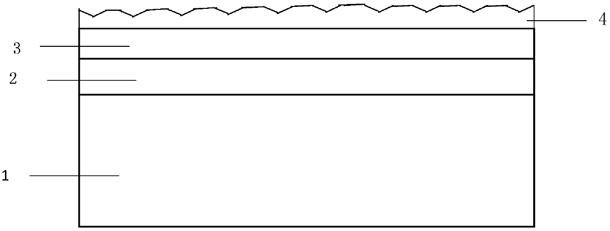
[0071] (1) On the GaAs substrate 1, the heavily doped N-type layer 2 and the quantum well layer 3 are grown sequentially, and the P-type layer 4 of the epitaxial wafer is roughened: using a mixed solution of HF, HNO3 and CH3COOH, the volume ratio of each substance is 3:2: 4. The temperature of the corrosive solution is 25-35°C, and the soaking time of the solution is 30-120s. Such as figure 1 shown.

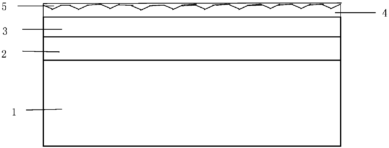
[0072] (2) On the roughened P-type layer 4 surface, prepare ITO film 5, SiO 2 Thin film, ITO thin film 5 thickness SiO 2 membrane thickness Such as figure 2 shown.

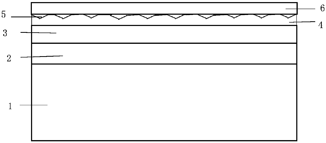
[0073] (3) Mix low-temperature glass powder and high-purity water into a paste, and apply it to the surface of the P-type layer 4 formed in step (2). The thickness of the glass powder is controlled at 1-2mm, and the furnace tube can be used to heat, and the furnace tube can maintain a low vacuum state, according to ...

Embodiment 2

[0084] A method for preparing a reverse polarity AlGaInP quaternary LED chip, comprising:

[0085] (1) On the GaAs substrate 1, the heavily doped N-type layer 2 and the quantum well layer 3 are sequentially grown, and the P-type layer 4 of the epitaxial wafer is roughened: using a mixed solution of HF, HNO3 and CH3COOH, wherein the volume ratio of each substance is 3:2 :4, the temperature of the corrosive solution is 25-35°C, and the soaking time of the solution is 30-120s.

[0086] (2) On the surface of the roughened P-type layer 4, prepare ITO film, SiO 2 film, where the thickness of the ITO film 5 SiO 2 membrane thickness

[0087] (3) Mix low-temperature glass powder and high-purity water into a paste, and apply it to the surface of the P-type layer 4 formed in step (2). The thickness of the glass powder is controlled at 1-2mm, and the furnace tube can be used to heat, and the furnace tube can maintain a low vacuum state, according to the steps in Table 2 below, th...


PUM

PropertyMeasurementUnit
thicknessaaaaaaaaaa

Abstract

The invention relates to a preparation method of a reversed polarity AlGaInP quaternary LED chip. The preparation method comprises the following steps: (1) sequentially growing a heavily doped N-typelayer, a quantum well layer and a P-type layer on a substrate; (2) roughening the surface of the P-type layer; (3) preparing a transparent conductive film or a composite film on the surface of the P-type layer; (4) preparing a glass layer on the transparent conductive film or the composite film; (5) removing the substrate; (6) etching the heavily doped N-type layer, the quantum well layer and theP-type layer, and exposing the transparent conductive film or the composite film corresponding to the P electrode; (7) preparing a P electrode on the exposed transparent conductive film or composite film, and preparing an N electrode on the heavily doped N-type layer; (8) grinding the glass layer; (9) performing cutting to obtain the product. According to the invention, the low-temperature glass powder is utilized to form the light emitting layer, the light emitting layer is used as a substrate support and also used as a light emitting layer, and the process mode does not need high-pressure bonding and permanent substrate bonding.

Description

technical field [0001] The invention relates to a method for preparing a reverse polarity AlGaInP quaternary LED chip, which is suitable for preparing reverse polarity chips and miniled chips, and belongs to the field of optoelectronic technology. Background technique [0002] LED is a new light source for lighting in the 21st century. Under the same brightness, the power consumption of semiconductor lamps is only 1 / 10 of that of ordinary incandescent lamps, but the life span can be extended by 100 times. The LED device is a cold light source with high luminous efficiency, low working voltage, low power consumption, small size, flat packaging, easy to develop thin and light products, strong structure and long life. The light source itself does not contain harmful substances such as mercury and lead. No infrared and ultraviolet pollution, no pollution to the outside world during production and use. Therefore, semiconductor lamps have the characteristics of energy saving, env...

Claims


Application Information

Patent Timeline
Patent Type & Authority Applications(China)
IPC IPC(8): H01L33/00H01L33/22
CPCH01L33/0062H01L33/22
Inventor 彭璐张兆梅厉夫吉王成新
Owner SHANDONG INSPUR HUAGUANG OPTOELECTRONICS
Learn More