Semiconductor device and manufacturing method thereof

A manufacturing method and semiconductor technology, which are applied in the fields of semiconductor/solid-state device manufacturing, semiconductor devices, semiconductor/solid-state device components, etc., can solve the problems of increasing the threshold voltage of IGBT transistors, affecting the performance of semiconductor devices, and enhancing impurity doping concentration, etc. Achieve the effect of improving thickness consistency, ensuring depth consistency, and reducing production costs

Inactive Publication Date: 2020-01-10
SEMICON MFG ELECTRONICS (SHAOXING) CORP
View PDF4 Cites 0 Cited by
  • Summary
  • Abstract
  • Description
  • Claims
  • Application Information

AI Technical Summary

Problems solved by technology

[0004] With the continuous reduction of device size, the size of the active region needs to be continuously reduced, and the critical dimension (CD size) reserved for the contact hole and gate trench at the design end is also gradually reduced. The process process inevitably needs to consider the alignment accuracy with the gate trench. Therefore, for small-sized device structures, the fluctuation between proc

Method used


Image

  • Semiconductor device and manufacturing method thereof
  • Semiconductor device and manufacturing method thereof
  • Semiconductor device and manufacturing method thereof

Examples


Example Embodiment

[0035] In order to make the purpose, advantages and features of the present invention clearer, the technical solution proposed by the present invention will be further described in detail below with reference to the accompanying drawings. It should be noted that the drawings are in a very simplified form and all use imprecise proportions, which are only used to conveniently and clearly assist in explaining the purpose of the embodiments of the present invention.
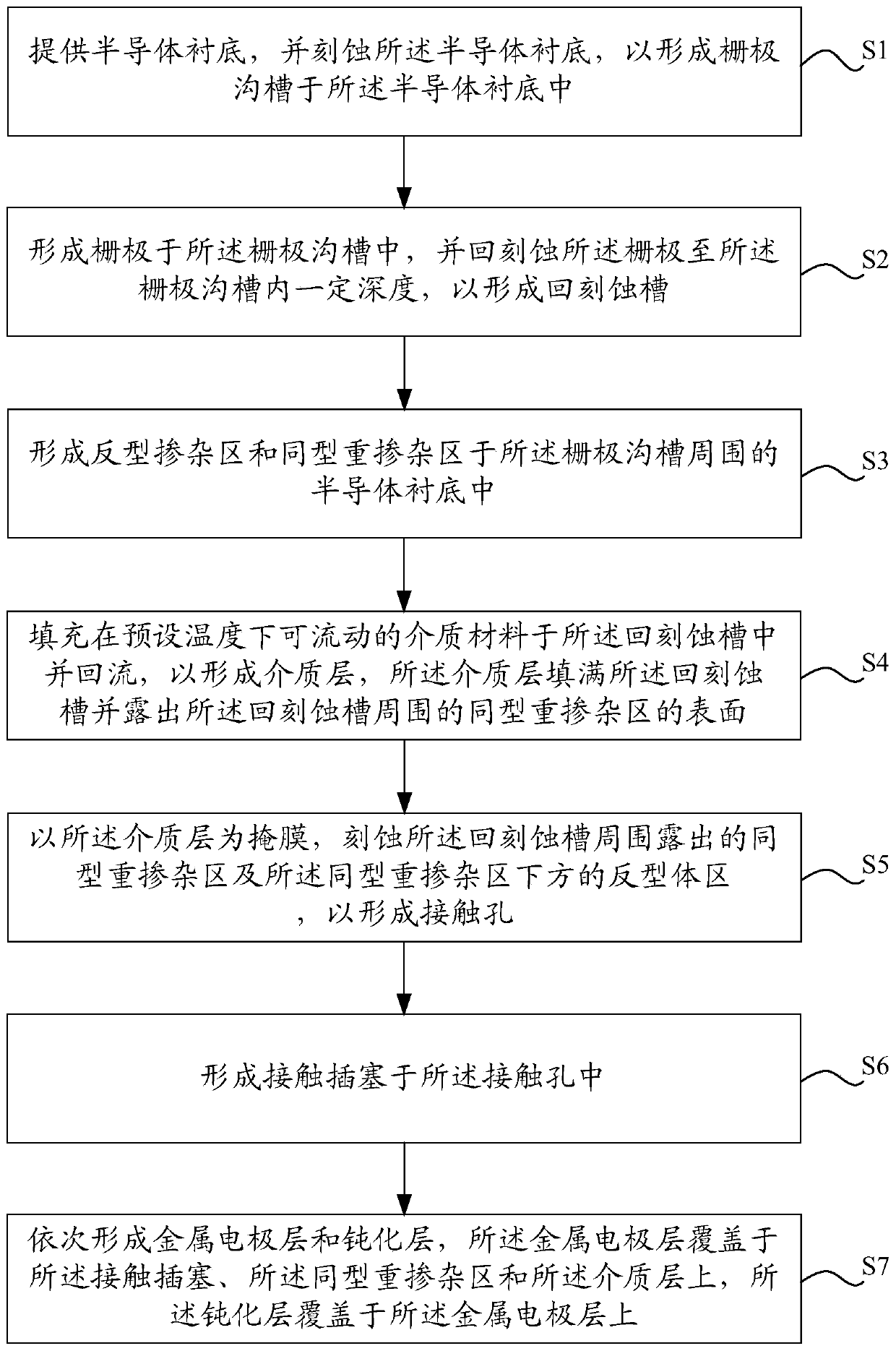
[0036] Please refer to figure 1 , The present invention provides a method for manufacturing a semiconductor device, including the following steps:

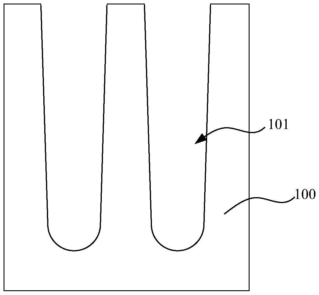
[0037] S1, providing a semiconductor substrate, and etching the semiconductor substrate to form a gate trench in the semiconductor substrate;

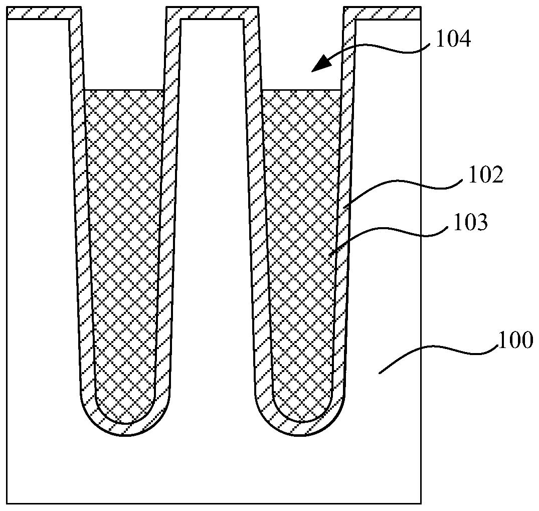
[0038] S2, forming a gate in the gate trench, and etch back the gate to a certain depth in the gate trench to form an etch-back groove;

[0039] S3, forming an inversion doped region and a homotype heavily doped region in the semiconduct...


PUM


Abstract

The invention provides a semiconductor device and a manufacturing method thereof. The method takes a dielectric layer as a mask and etches and a same-type heavily-doped region around a back-etched groove and a partial thickness of opposite-type body region under the same-type heavily-doped region to form a contact hole with a required depth. The method is substantially a self-aligning contact holeetching process, so that the problem of contact hole alignment offset caused by process fluctuation is basically solved, it is ensured that the contact hole and a gate trench have very high alignmentprecision, the problem that impurity ions injected into the contact hole are diffused to a channel region after annealing in the later process is avoided, and the performance of the semiconductor device is improved. Besides, since the method is the self-aligning contact hole etching process, the contact hole can be etched without the assistance of a photomask plate, so that one photomask plate can be saved, and the production cost is reduced.

Description

technical field [0001] The invention relates to the technical field of semiconductor manufacturing, in particular to a semiconductor device and a manufacturing method thereof. Background technique [0002] At present, the technology of IGBT (Insulated Gate Bipolar Transistor, insulated gate bipolar transistor) and VDMOS (Vertical Double-diffused MOSFET, vertical channel double-diffused metal oxide transistor) is constantly innovating, and the size of power semiconductor devices is constantly being realized. Under the premise of shrinking, the excellent performance of power semiconductor devices is also guaranteed. [0003] In the manufacturing process of the existing trench type IGBT transistor, it is necessary to transfer the design pattern of the contact hole from the mask plate to the wafer by means of a photolithography process after the trench type gate is completed, but when transferring the pattern , it is necessary to align the lithography alignment mark on the mask...

Claims


Application Information

Patent Timeline
IPC IPC(8): H01L21/768H01L21/8222H01L21/8234H01L23/48H01L27/082H01L27/088
CPCH01L21/76897H01L21/8222H01L21/823437H01L21/823475H01L23/481H01L27/0823H01L27/088
Inventor 王珏陈政周旭钟荣祥眭小超
Owner SEMICON MFG ELECTRONICS (SHAOXING) CORP
Why Eureka
Try Eureka