Superconducting nanowire single-photon detector array capable of distinguishing photon energy
A single-photon detector and superconducting nanowire technology, which is applied to superconductor components and instruments, can solve the problem of not having the ability to distinguish different photon energies or light wavelengths, solve the problem of multi-channel cooperative work, and broaden the application range effect
- Summary
- Abstract
- Description
- Claims
- Application Information
AI Technical Summary
Problems solved by technology
Method used
Image
Examples
Embodiment 1
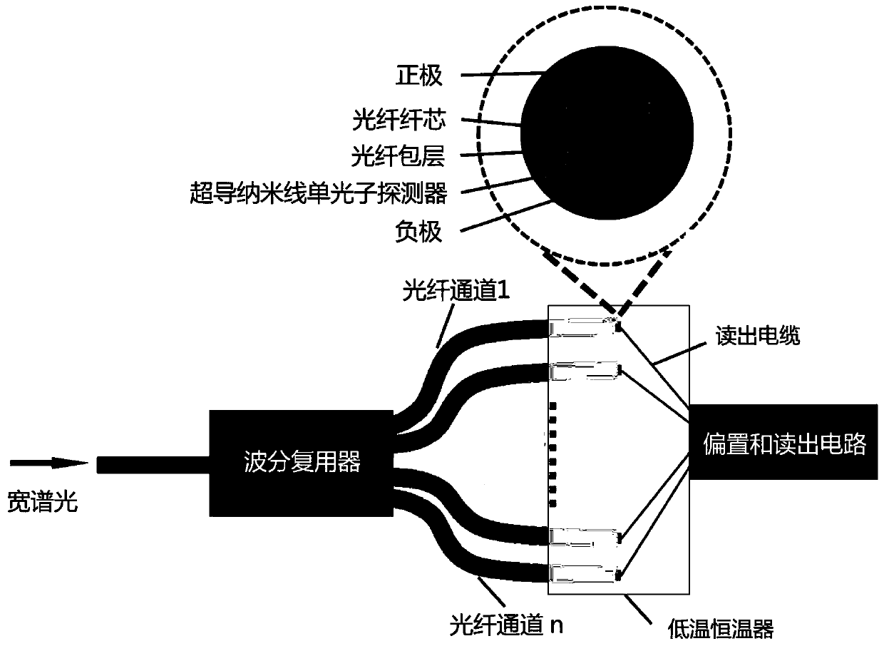
[0035] Embodiment 1 The overall technical scheme of the invention is as figure 1 Shown: a beam of broad-spectrum light is incident from the left end of the fiber, and after passing through the fiber wavelength division multiplexer, light with different photon energy (wavelength) is output from different fiber channels (fiber channel 1.....fiber channel n) on the right end , And connected to a cryostat; in the cryostat, a superconducting nanowire single-photon detector is printed on the terminal end of each optical fiber. The superconducting nanowire single-photon detector covers the fiber core, and the anode and cathode are set on the fiber On the end face of the cladding layer, the readout cable is connected with the positive electrode and the negative electrode; the superconducting nanometer single photon detector is connected in the bias and readout circuit to read the photon count rate.
[0036] Therefore, a superconducting nanowire single-photon detector array capable of dist...
Embodiment approach
[0050] The best implementation plan is as follows:
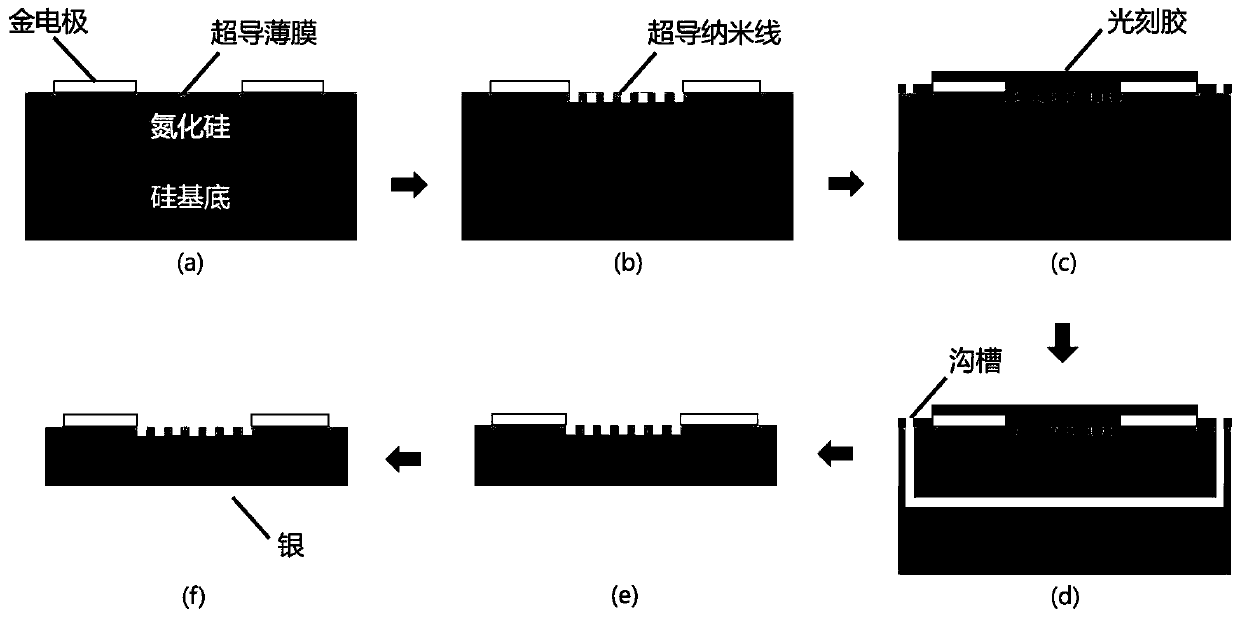
[0051] 1. Processing superconducting nanowire single-photon detectors based on thin films
[0052] A layer of silicon nitride with a certain thickness is grown by plasma enhanced chemical vapor deposition, and a layer of superconducting film material with a certain thickness is sputtered on the silicon nitride by magnetron sputtering, and gold is processed on the superconducting film electrode;
[0053] Transfer the nanowire pattern to the electron beam exposure glue through the electron beam exposure method, use the electron beam exposure glue as a mask, and etch the nanowire pattern by the reactive ion beam etching method;
[0054] The etching window is opened by photolithography, the silicon is etched and the superconducting nanowire single-photon detector is removed from the film, and the silicon substrate is plated with silver.
[0055] 2. Make a titanium gold electrode on the fiber end face on the right side of the wavelength d...
PUM
 Abstract
Description
Claims
Application Information
 - R&D
- Intellectual Property
- Life Sciences
- Materials
- Tech Scout
- Unparalleled Data Quality
- Higher Quality Content
- 60% Fewer Hallucinations
Browse by: Latest US Patents, China's latest patents, Technical Efficacy Thesaurus, Application Domain, Technology Topic, Popular Technical Reports.
© 2025 PatSnap. All rights reserved.Legal|Privacy policy|Modern Slavery Act Transparency Statement|Sitemap|About US| Contact US: help@patsnap.com


