Barrier adjustment method for silicon carbide Schottky diode

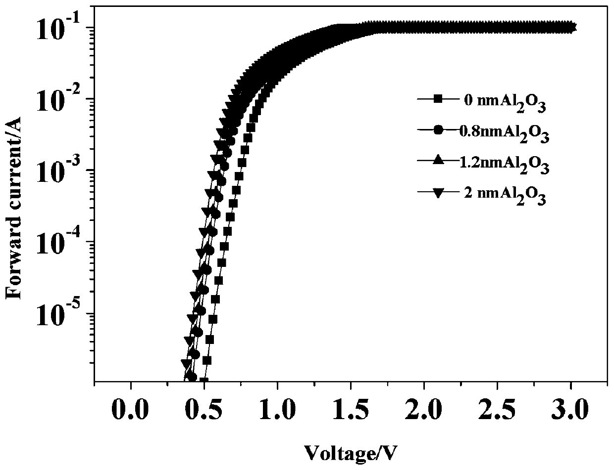
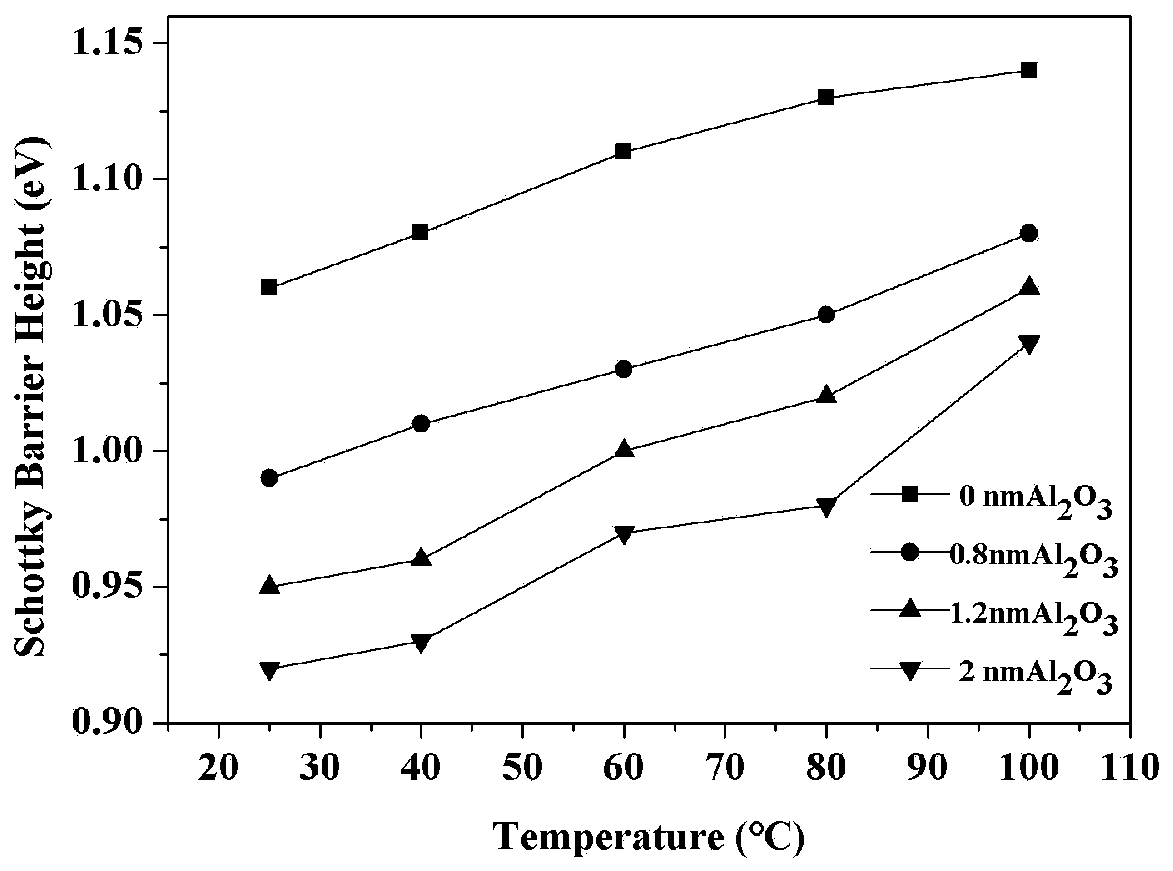
A technology of Schottky diodes and adjustment methods, applied in electrical components, circuits, semiconductor devices, etc., can solve the problems of low forward voltage drop, unsatisfactory, low Schottky barrier height, etc., and reduce power consumption of devices. Small, reduce forward voltage drop, achieve the effect of adjustability

Inactive Publication Date: 2020-01-24
HANGZHOU DIANZI UNIV
View PDF6 Cites 0 Cited by
  • Summary
  • Abstract
  • Description
  • Claims
  • Application Information

AI Technical Summary

Problems solved by technology

[0004] Ti has low Schottky barrier height (SBH) as well as low forward voltage drop, but some unfavorable I-V characteristics tend to appear in Ti / SiC SBDs due to interface state, contamination caused by residual processing, inhomogeneity The impact of incomplete SBH, and the existing redemption to improve the interface unevenness and obtain a lower Schottky barrier height generally adopts heat treatment, but the heat treatment method cannot avoid silicidation and thermal budget, resulting in device power consumption and operating costs high

Method used


Image

  • Barrier adjustment method for silicon carbide Schottky diode
  • Barrier adjustment method for silicon carbide Schottky diode
  • Barrier adjustment method for silicon carbide Schottky diode

Examples


Embodiment Construction

[0016] The following will clearly and completely describe the technical solutions in the embodiments of the present invention with reference to the accompanying drawings in the embodiments of the present invention. Obviously, the described embodiments are only some, not all, embodiments of the present invention. Based on the embodiments of the present invention, all other embodiments obtained by persons of ordinary skill in the art without making creative efforts belong to the protection scope of the present invention.

[0017] In order to make the above objects, features and advantages of the present invention more comprehensible, the present invention will be further described in detail below in conjunction with the accompanying drawings and specific embodiments.

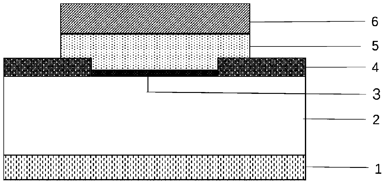
[0018] refer to Figure 1-3 , the preparation method of silicon carbide Schottky contact, comprises the following steps:

[0019] Step 1, perform standard RCA cleaning on the 4H-SiC substrate and epitaxial layer ...


PUM

PropertyMeasurementUnit
thicknessaaaaaaaaaa
thicknessaaaaaaaaaa
thicknessaaaaaaaaaa

Abstract

The invention discloses a barrier adjustment method for a silicon carbide Schottky diode. According to the method, a layer of Al2O3 film is inserted into a Ti/4H-SiC Schottky diode, and therefore, interface non-uniformity can be improved, and the height of a barrier can be adjusted. The Al2O3 thin film layer with different thicknesses is grown on an atomic layer through deposition before metal Tiis sputtered, subsequently, Al2O3 reacts with silicon carbide, so that a dipole layer can be formed, potential difference between two sides of an interface is caused, and therefore, the height of a Schottky barrier is reduced, and the power consumption of the device is reduced; the Al2O3 film and the silicon carbide can generate a positive barrier, and therefore the reverse leakage current of theSchottky diode can be reduced; the thicknesses of the Al2O3 thin film layer can be differently adjusted, so that different barrier heights are generated, and therefore, the adjustability of the heightof the barrier is realized.

Description

technical field [0001] The invention belongs to the technical field of microelectronic devices, and relates to a method for adjusting the potential barrier of a Schottky diode of the third-generation wide bandgap semiconductor material 4H-SiC. Background technique [0002] Compared with ordinary P-N junction diodes, Schottky diodes (SBDs) have the advantages of reduced forward voltage, short reverse recovery time and strong anti-surge current capability, etc., and are used in high-speed and high-efficiency rectifier circuits, microwave circuits and in high-speed integrated circuits. Schottky diodes use a metal as the positive electrode, the metal is selected from Au, Ag, Al, Pt, Mo, Ni, Ti, and an N-type semiconductor as the negative electrode, and the semiconductor is SiC. A metal-semiconductor device made of a barrier with rectifying properties. [0003] Today's semiconductor devices are constantly advancing in the direction of high energy and low price, and the process ...

Claims


Application Information

Patent Timeline
Patent Type & Authority Applications(China)
IPC IPC(8): H01L29/47H01L21/329H01L29/872
CPCH01L29/47H01L29/872H01L29/66143
Inventor 王颖时定坤曹菲于成浩包梦恬
Owner HANGZHOU DIANZI UNIV
Why Eureka
Try Eureka