A Longitudinal Tunneling Field Effect Transistor with Improved Subthreshold Swing

A tunneling field effect, sub-threshold swing technology, applied in semiconductor devices, electrical components, circuits, etc., can solve the problems of sub-threshold characteristics of devices, etc., to improve on-state current, increase leakage current, and circuit design. Flexibility-enhancing effects

Active Publication Date: 2021-04-27
UNIV OF ELECTRONICS SCI & TECH OF CHINA
View PDF8 Cites 0 Cited by
  • Summary
  • Abstract
  • Description
  • Claims
  • Application Information

AI Technical Summary

Problems solved by technology

[0007] The purpose of the present invention is to solve the current heterojunction TFET devices, especially when SiGe narrow bandgap material is used to improve the on-state current of TFET, two tunneling regions occur successively due to the energy band mismatch between the silicon germanium material and the silicon material. Tunneling, which causes the problem of deteriorating subthreshold characteristics of the device, provides a longitudinal tunneling field effect transistor with improved subthreshold swing

Method used


Image

  • A Longitudinal Tunneling Field Effect Transistor with Improved Subthreshold Swing
  • A Longitudinal Tunneling Field Effect Transistor with Improved Subthreshold Swing
  • A Longitudinal Tunneling Field Effect Transistor with Improved Subthreshold Swing

Examples


Embodiment 1

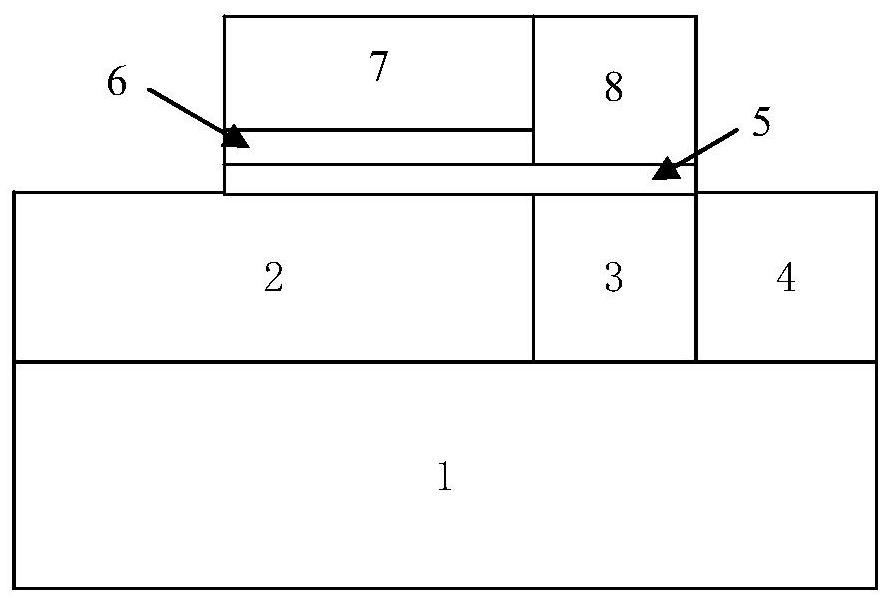
[0045] A longitudinal tunneling field effect transistor with improved sub-threshold swing according to Embodiment 1 of the present invention, its cross-sectional view can be found in figure 1 , including a semiconductor substrate 1, a source region 2, an intrinsic region 3, a drain region 4, an epitaxial region 5, a gate oxide layer 6, a metal gate 7 and a gate spacer 8, to make an N-type substrate on a P-type substrate Take TFETs as an example.

[0046] Its production process is as follows:

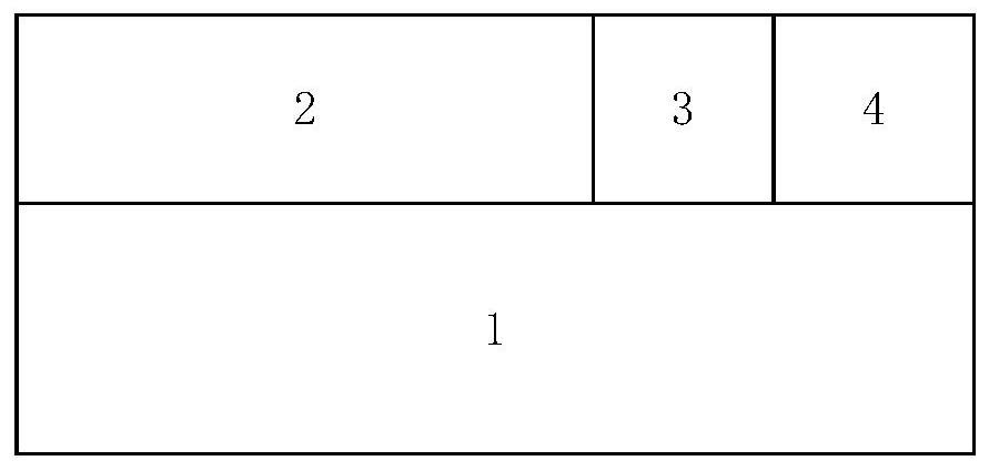
[0047] Step 1: Select the doping concentration as light doping (10 14 ~10 16 cm -3 ) of P-type single crystal silicon as the material of the semiconductor substrate 1, see figure 2 ;

[0048] Step 2: Using an ion implantation process to form mutually independent P ++ type source region 2 and N + Type drain region 4, the region of substrate 1 between source region 2 and drain region 4 forms intrinsic region 3, see image 3 ;

[0049] Step 3: epitaxially grow a thin SiGe epitaxia...

Embodiment 2

[0058] Embodiment 2 of the present invention is a vertical heterojunction tunneling field effect transistor in which the material of the epitaxial region 5 is InAs, and its cross-sectional view can be found in figure 1 , including a semiconductor substrate 1, a source region 2, an intrinsic region 3, a drain region 4, an epitaxial region 5, a gate oxide layer 6, a metal gate 7 and a gate spacer 8, to make an N-type substrate on a P-type substrate Take TFETs as an example. The difference from the fabrication of the first embodiment is that the material of the epitaxial region 5 in the first embodiment is SiGe, and the material of the epitaxial region 5 in this embodiment is InAs.

[0059] Both InAs in Embodiment 2 and SiGe in Embodiment 1 are narrow bandgap materials. The electron affinity of the InAs material is 4.9eV, and the band gap is 0.354eV; the electron affinity of the Si material is 4.05eV, and the band gap is 1.12eV. It can be seen that the valence band positions of ...

Embodiment 3

[0061] Embodiment 3 of the present invention is a complementary vertical tunneling field effect transistor based on a gradually doped epitaxial region. Similar to CMOS, using the proposed gradient doped TFET structure, by adding a small number of masks and only changing the doping type of the corresponding region, N-TFET devices and P-TFET devices can be fabricated on the same substrate to achieve complementary longitudinal tunneling. Through the field effect transistor (TFET), its cross-section see Figure 14 , including semiconductor substrate 1, source region 2, intrinsic region 3, drain region 4, epitaxial region 5, gate oxide layer 6, metal gate 7, sidewall 8, shallow trench isolation STI9, P-epitaxial layer 10, passivation Layer 11 and metal tungsten 12, the production process is as follows:

[0062] Step 1: Select highly doped P-type single crystal silicon (Si) as the material of the semiconductor substrate 1, the resistivity of the semiconductor substrate 1 is 0.009-0...


PUM

PropertyMeasurementUnit
thicknessaaaaaaaaaa
widthaaaaaaaaaa
electron work functionaaaaaaaaaa

Abstract

The present invention relates to semiconductor technology. The invention solves the problem that in the existing heterojunction TFET devices, especially when the SiGe narrow bandgap material is used to increase the on-state current of the TFET, the two tunneling regions successively occur due to the energy band mismatch between the silicon germanium material and the silicon material. wear, resulting in the deterioration of the sub-threshold characteristics of the device, a longitudinal tunneling field-effect transistor with improved sub-threshold swing is provided, and the technical solution can be summarized as: a longitudinal tunneling field-effect transistor with improved sub-threshold swing , including a source region, an intrinsic region, a drain region, an epitaxial region, a gate and a gate spacer, the gate comprises a gate oxide layer and a metal gate, the epitaxial region adopts a narrow band gap material, and the doping of the epitaxial region The concentration in the epitaxial region shows a gradual change from high to low from the interface contacting the source region to the interface contacting the gate oxide layer. The beneficial effect of the present invention is that the sub-threshold characteristic is improved, and it is suitable for vertical tunneling field effect transistors.

Description

technical field [0001] The invention relates to semiconductor technology, in particular to a tunneling field effect transistor (TFET, Tunneling Field Effect Transistor). Background technique [0002] With the continuous shrinking of the feature size of traditional MOSFET devices and the gradual increase of chip integration, the short-channel effect of devices has become more and more obvious, resulting in a significant increase in leakage current when the device is turned off, and the problem of power consumption is becoming more and more serious, which is not conducive to Further improvement of chip integration. The subthreshold swing of traditional MOSFETs at room temperature is higher than 60mV / dec due to the carrier drift diffusion working principle, resulting in high off-state current; and the tunneling field effect transistor (TFET) based on quantum tunneling effect, its subthreshold The slope can break through the theoretical limit of the subthreshold swing of MOSFET...

Claims


Application Information

Patent Timeline
Patent Type & Authority Patents(China)
IPC IPC(8): H01L29/78H01L29/423
CPCH01L29/4238H01L29/785
Inventor 王向展陈玉翔刘洋于奇
Owner UNIV OF ELECTRONICS SCI & TECH OF CHINA
Why Eureka
Try Eureka