Vertical Tunneling Field Effect Transistor with Enhanced On-state Current

A tunneling field effect and on-state current technology, applied in circuits, electrical components, semiconductor devices, etc., can solve problems such as poor performance of TFET devices, and achieve enhanced device on-state current, increased tunneling probability, and increased electric field. The effect of line density

Active Publication Date: 2021-01-29
UNIV OF ELECTRONICS SCI & TECH OF CHINA
View PDF7 Cites 0 Cited by
  • Summary
  • Abstract
  • Description
  • Claims
  • Application Information

AI Technical Summary

Problems solved by technology

[0007] The purpose of the present invention is to overcome the shortcomings of poor performance of current TFET devices and provide a vertical tunneling field effect transistor with enhanced on-state current

Method used


Image

  • Vertical Tunneling Field Effect Transistor with Enhanced On-state Current
  • Vertical Tunneling Field Effect Transistor with Enhanced On-state Current
  • Vertical Tunneling Field Effect Transistor with Enhanced On-state Current

Examples


Embodiment 1

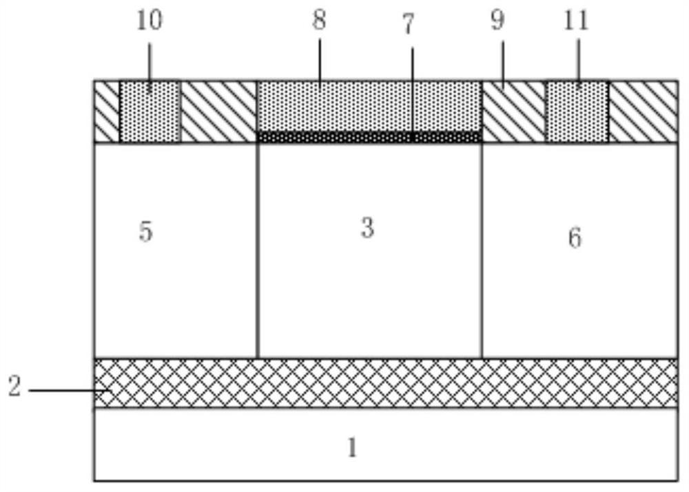
[0038] The vertical tunneling field-effect transistor with enhanced on-state current in Embodiment 1 of the present invention, its cross-sectional view can be found in image 3 , including a semiconductor substrate 1, a buried oxide layer 2, an intrinsic region 3, a source region 5, a drain region 6, a gate oxide layer 7, a gate electrode 8, sidewalls 9, a source electrode 10, a drain electrode 11 and a low-K dielectric region 4. Wherein, the buried oxide layer 2 is arranged above the semiconductor substrate 1, and its lower surface is in contact with the upper surface of the semiconductor substrate 1, and the low-K dielectric layer 4, the intrinsic region 3 and the drain region 6 are respectively arranged on the buried oxide layer 2, the lower surface of the low-K dielectric layer 4, the lower surface of the intrinsic region 3, and the lower surface of the drain region 6 are respectively in contact with the upper surface of the buried oxide layer 2, and the two sides of the in...

Embodiment 2

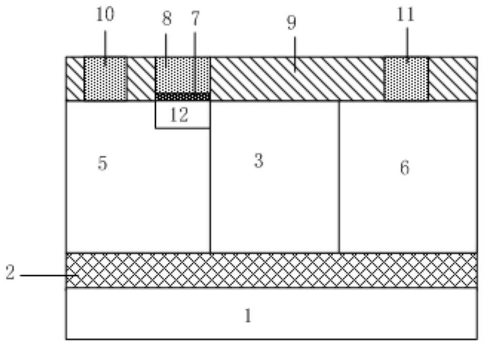
[0053] The vertical tunneling field-effect transistor with enhanced on-state current in Embodiment 2 of the present invention, its cross-sectional view can be found in Figure 4 , which differs from Embodiment 1 only in that the low-K dielectric region 4 adopts a vacuum with a relative permittivity of 1, which is less than the relative permittivity of silicon dioxide, 3.9, and less than the relative permittivity of silicon, 11.2. As for the vacuum medium area, it can be produced by a suitable method, and other processes are basically the same. Through simulation verification, it can be seen that under the same other conditions, the smaller the dielectric constant of the insulating material in the low-K dielectric region 4 is, the better the performance of the resulting device is. As far as the material of the low-K dielectric region 4 is concerned, the electric field enhancement effect is the best when a vacuum is used.

Embodiment 3

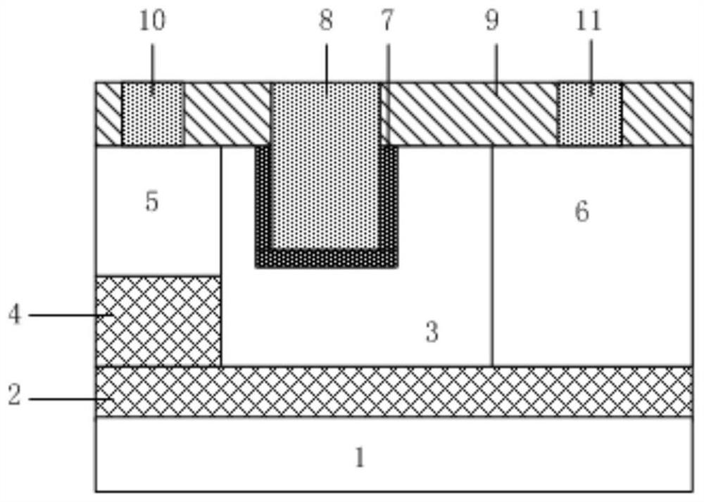
[0055] The on-state current-enhanced vertical tunneling field effect transistor in Embodiment 3 of the present invention, its cross-sectional view can be found in Figure 5, the difference from Embodiment 1 is only that: the SOI silicon wafer for making the device is replaced by a common non-SOI silicon wafer, so that the materials of the semiconductor substrate 1 and the buried oxide layer 2 are the same as those of the intrinsic region 3, and other processes are basically the same . Since the price of ordinary silicon wafers is much lower than that of SOI silicon wafers, device manufacturing costs can be reduced. At the same time, the advantages of strong gate control ability, large tunneling area, and low-K dielectric region 4 are helpful to increase the tunneling electric field under the tunneling junction and reduce device leakage. However, the advantages of increased tunneling junction electric field and reduced leakage obtained by devices on ordinary silicon wafers wil...


PUM

PropertyMeasurementUnit
thicknessaaaaaaaaaa
thicknessaaaaaaaaaa
relative permittivityaaaaaaaaaa

Abstract

The invention relates to small-scale tunneling field effect transistor technology. The present invention solves the problem of poor performance of existing TFET devices, and provides a longitudinal tunneling field effect transistor with enhanced on-state current, and its technical solution can be summarized as: a longitudinal tunneling field effect transistor with enhanced on-state current, and The difference in the prior art is that a low-K dielectric region is provided between the source region and the buried oxide layer, a part of the gate electrode is embedded in the intrinsic region, and there is a gate oxide layer between the gate electrode and the intrinsic region. The beneficial effect of the invention is that the tunneling probability is improved, the on-state current of the device is increased, and it is suitable for small-sized tunneling field effect transistors.

Description

technical field [0001] The invention belongs to the field of CMOS ultra-large-scale integrated circuits, and in particular relates to small-size tunneling field effect transistor (TFET, Tunneling Field Effect Transistor) technology. Background technique [0002] Under the strong impetus of Moore's Law, with the improvement of ion implantation, lithography and etching technologies in semiconductor technology, the traditional MOSFET (Metal-Oxide-Semiconductor Field-Effect Transistor, Metal-Oxide-Semiconductor Field-Effect Transistor) The feature size of integrated circuit chips is gradually reduced, and the degree of integration is gradually increased. However, with the improvement of chip performance, the problem of power consumption is becoming more and more serious. While devices are scaled down, problems such as device short-channel effects, quantum tunneling effects, drain-induced barrier reduction, and gate-induced drain leakage currents have seriously hindered the devel...

Claims


Application Information

Patent Timeline
Patent Type & Authority Patents(China)
IPC IPC(8): H01L29/08H01L29/10H01L29/423H01L21/336H01L29/78
Inventor 王向展陆世丁曹雷李竞春于奇
Owner UNIV OF ELECTRONICS SCI & TECH OF CHINA
Why Eureka
Try Eureka