Thin-film capacitor
A thin-film capacitor and thin-film technology, applied in the energy field, can solve problems such as the decrease in the bonding force between electrodes and ceramic thin films, and achieve high reliability, good energy storage performance, and low dielectric loss
- Summary
- Abstract
- Description
- Claims
- Application Information
AI Technical Summary
Problems solved by technology
Method used
Image

Examples
preparation example Construction
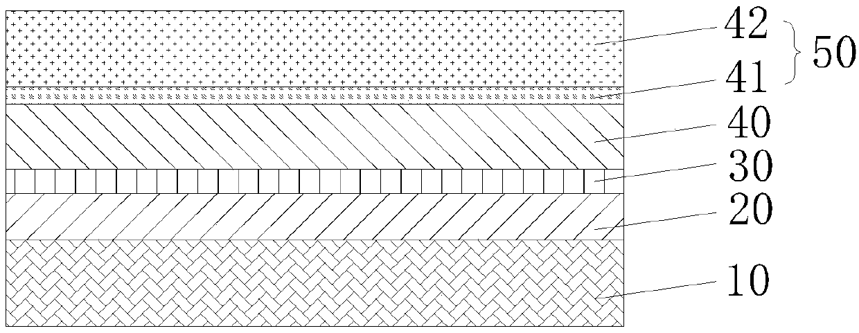
[0023] The preparation method of the energy storage ceramic thin film provided by the present invention comprises:
[0024] S1, providing a metal substrate;
[0025] S2, using the first simple metal as the first target material, depositing a first metal prefabricated layer on the metal substrate by using a magnetic filter multi-arc ion plating method, the material of the first metal prefabricated layer is compatible with the metal substrate The material of the bottom is the same;
[0026] S3, using the second metal simple substance as the second target material, depositing a second metal prefabricated layer on the first metal prefabricated layer by using a magnetic filter multi-arc ion plating method, and while depositing and forming the second metal prefabricated layer, An alloy prefabricated layer is formed between the first metal prefabricated layer and the second metal prefabricated layer, and the alloy prefabricated layer is an alloy formed by the first metal and the sec...
Embodiment 1
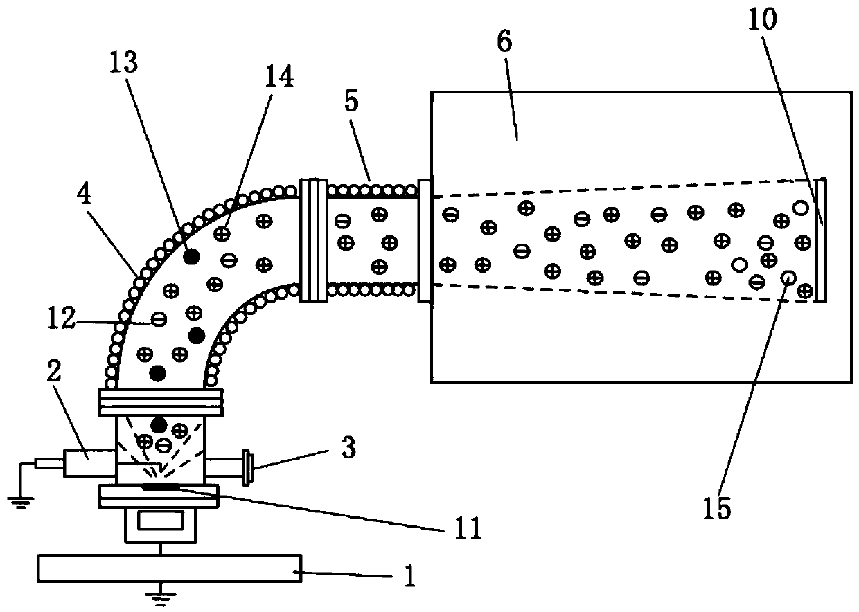
[0071] With a flexible low-roughness copper foil as the substrate, the thickness is 6 μm, the surface roughness is 10 nm, placed in a vacuum chamber, and evacuated to 3×10 -3 Pa. The vacuum chamber is heated to 150°C, the holding time is 10min, filled with argon, the flow rate of argon is 20sccm, and the vacuum degree of the vacuum chamber is 2×10 -2 Pa, turn on the Hall ion source, set the voltage of the Hall ion source to 1000V, the current to 0.5A, and treat for 1min to make the surface tension of the copper foil reach 60 dynes.
[0072] Maintain a vacuum of 2.0×10 -2 Pa, the argon gas flow rate is 20sccm, using metal copper as the target material, turn on the first magnetic filter multi-arc ion plating power supply, adjust the arc current to 50A, draw the current 9A, apply the bias voltage to the copper foil to 5V, and the deposition time is 35s, A copper prefabricated layer with a thickness of 35 nm is formed on the copper foil, and the first magnetic filter multi-arc i...
Embodiment 2
[0079] With a flexible low-roughness copper foil as the substrate, the thickness is 10 μm, the surface roughness is 20 nm, placed in a vacuum chamber, and vacuumed to 3×10 -3 Pa. The vacuum chamber is heated to 100°C, the holding time is 20min, filled with argon, the flow rate of argon is 30sccm, and the vacuum degree of the vacuum chamber is 3×10 -2 Pa, turn on the Hall ion source, set the voltage of the Hall ion source to 800V, and the current to 0.6A, and treat for 5min to make the surface tension of the copper foil reach 65 dynes.
[0080] Maintain a vacuum of 3.0×10 -2 Pa, the argon gas flow rate is 30sccm, and the metal copper is used as the target material. Turn on the first magnetic filter multi-arc ion plating power supply, adjust the arc current to 55A, draw the current to 10A, apply the bias voltage to the copper foil to 6V, and deposit for 45s. A copper prefabricated layer with a thickness of 45 nm is formed on the copper foil, and the first magnetic filter multi...
PUM
| Property | Measurement | Unit |
|---|---|---|
| Surface roughness | aaaaa | aaaaa |
| Thickness | aaaaa | aaaaa |
| Thickness | aaaaa | aaaaa |
Abstract
Description
Claims
Application Information
 - R&D Engineer
- R&D Manager
- IP Professional
- Industry Leading Data Capabilities
- Powerful AI technology
- Patent DNA Extraction
Browse by: Latest US Patents, China's latest patents, Technical Efficacy Thesaurus, Application Domain, Technology Topic.
© 2024 PatSnap. All rights reserved.Legal|Privacy policy|Modern Slavery Act Transparency Statement|Sitemap