Processing method of silicon base substrate

A processing method and substrate technology, which are applied in the manufacturing of electrical components, circuits, semiconductor/solid-state devices, etc., can solve the problems of device process difficulty and large flatness of epitaxial materials.

Active Publication Date: 2022-04-15
11TH RES INST OF CHINA ELECTRONICS TECH GROUP CORP
View PDF6 Cites 0 Cited by
  • Summary
  • Abstract
  • Description
  • Claims
  • Application Information

AI Technical Summary

Problems solved by technology

However, due to the problem of excessive flatness of the epitaxial material, it has caused great difficulty in the device process

Method used


Image

  • Processing method of silicon base substrate
  • Processing method of silicon base substrate
  • Processing method of silicon base substrate

Examples


Embodiment Construction

[0034] In order to further explain the technical means and functions adopted by the present invention to achieve the intended purpose, the present invention will be described in detail below in conjunction with the accompanying drawings and preferred embodiments.

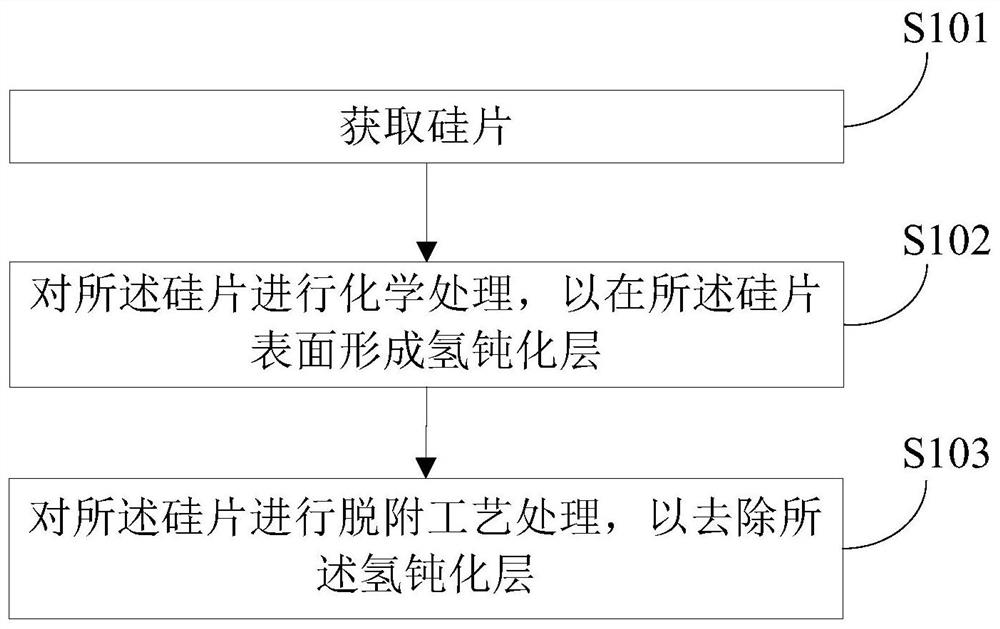
[0035] A high-quality Si-based CdTe composite substrate is an important prerequisite for the preparation of Si-based HgCdTe materials. In related technologies, the Si wafer epitaxial material needs to be wet chemically cleaned to remove the dense oxide layer on the surface, and then form a new oxide layer. The natural oxide layer on the surface of the Si sheet is relatively dense, and it needs to be heated above 1000°C in the MBE system to desorb. However, under such high temperature conditions, the Si sheet is easily damaged and new impurities will be introduced.

[0036] The new oxide layer after wet chemical treatment has only 1-2 atomic layers, which is relatively easy to remove while protecting the surface of t...


PUM

PropertyMeasurementUnit
thicknessaaaaaaaaaa
warpageaaaaaaaaaa
surface smoothnessaaaaaaaaaa

Abstract

The invention proposes a method for processing a silicon-based substrate, comprising: obtaining a silicon wafer; chemically treating the silicon wafer to form a hydrogen passivation layer on the surface of the silicon wafer; performing a desorption process on the silicon wafer to remove hydrogen passivation layer. According to the silicon-based substrate processing method of the embodiment of the present invention, after the silicon wafer is chemically treated, a hydrogen passivation layer is formed on the surface of the silicon wafer, which can effectively protect the silicon wafer. Moreover, the desorption temperature of the hydrogen passivation layer is relatively low, thereby effectively reducing the problem of bending damage and introducing impurities caused by the high-temperature desorption of the passivation layer on the silicon wafer. Moreover, when selecting a silicon wafer, optimize the silicon Chip screening standards, thereby effectively reducing the flatness of silicon-based substrates, improving the processing quality of silicon-based substrates, and facilitating the processing of large area array devices.

Description

technical field [0001] The invention relates to the technical field of chip processing, in particular to a method for processing a silicon-based substrate. Background technique [0002] High-quality mercury cadmium telluride (HgCdTe) thin film materials are the basis for the preparation of high-performance mercury cadmium telluride infrared focal plane detectors. Traditional HgCdTe thin films are mainly based on cadmium zinc telluride (CdZnTe) single crystal materials. Liquid phase epitaxy (LPE ) or molecular beam epitaxy (MBE) and other methods for the preparation of HgCdTe thin film materials. With the development of the third-generation HgCdTe infrared focal plane technology in the direction of large-scale, high-performance, and double-multicolor, traditional CdZnTe-based HgCdTe materials are difficult to obtain large-area crystal materials due to the difficulty in growing CdZnTe bulk crystals. The disadvantages of CdZnTe substrate, such as low mechanical strength, poor ...

Claims


Application Information

Patent Timeline
Patent Type & Authority Patents(China)
IPC IPC(8): H01L21/30H01L21/02H01L21/311
CPCH01L21/3003H01L21/0206H01L21/31111
Inventor 王丛高达王经纬刘铭刘兴新于小兵周立庆
Owner 11TH RES INST OF CHINA ELECTRONICS TECH GROUP CORP
Why Eureka
Try Eureka