Embedded double-sided interconnection power module packaging structure and manufacturing method

A power module and packaging structure technology, which is applied in semiconductor/solid-state device manufacturing, electrical components, electric solid-state devices, etc., can solve problems such as power chip junction temperature rise, power module high heat, module error switching, etc., to reduce The effect of commutation circuit area, reduction of inductance of commutation circuit, and reduction of packaging volume

Active Publication Date: 2020-02-28
BEIJING UNIV OF TECH
View PDF5 Cites 10 Cited by
  • Summary
  • Abstract
  • Description
  • Claims
  • Application Information

AI Technical Summary

Problems solved by technology

However, this leads to an increase in the current density of the module, resulting in higher heat generation in the power module under service conditions
However, the traditional power module uses single-sided heat dissipation, and the heat can only be discharged from the collector of the IGBT power chip. This heat dissipation method has poor heat dissipation efficiency.
If the heat is not discharged in time, the junction temperature of the power chip will increase, and the higher junction temperature and junction temperature difference will affect the overall thermomechanical performance and reliability of the power module.
[0004] In addition, the traditional IGBT power module, due to the existence of the wire bonding interconnection structure, causes the module to generate a large parasitic inductance during operation. The existence of the parasitic inductance will cause electromagnetic interference between the chips and reduce the switching speed of the module. And the module has the risk of false switching
Therefore, the application of the module in high frequency conditions is limited

Method used


Image

  • Embedded double-sided interconnection power module packaging structure and manufacturing method
  • Embedded double-sided interconnection power module packaging structure and manufacturing method
  • Embedded double-sided interconnection power module packaging structure and manufacturing method

Examples


Embodiment Construction

[0052] In order to make the present invention more obvious and understandable, the specific implementation manners of the present invention will be described in detail below in conjunction with the accompanying drawings. For convenience of description, the components in the structures in the drawings of the embodiments are not scaled according to the normal scale, so they do not represent the actual relative sizes of the structures in the embodiments.

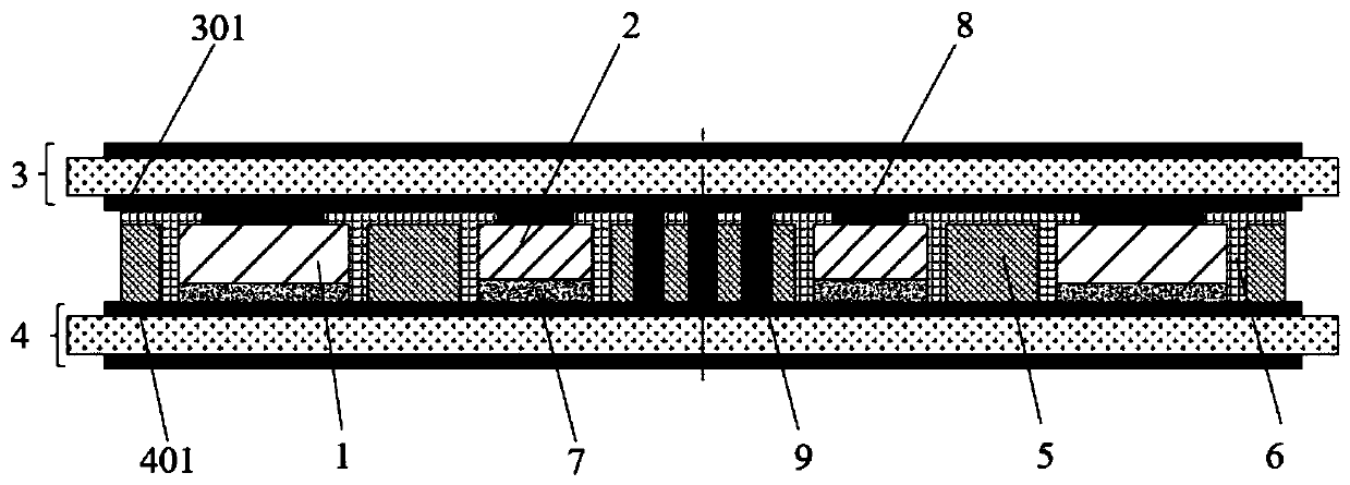
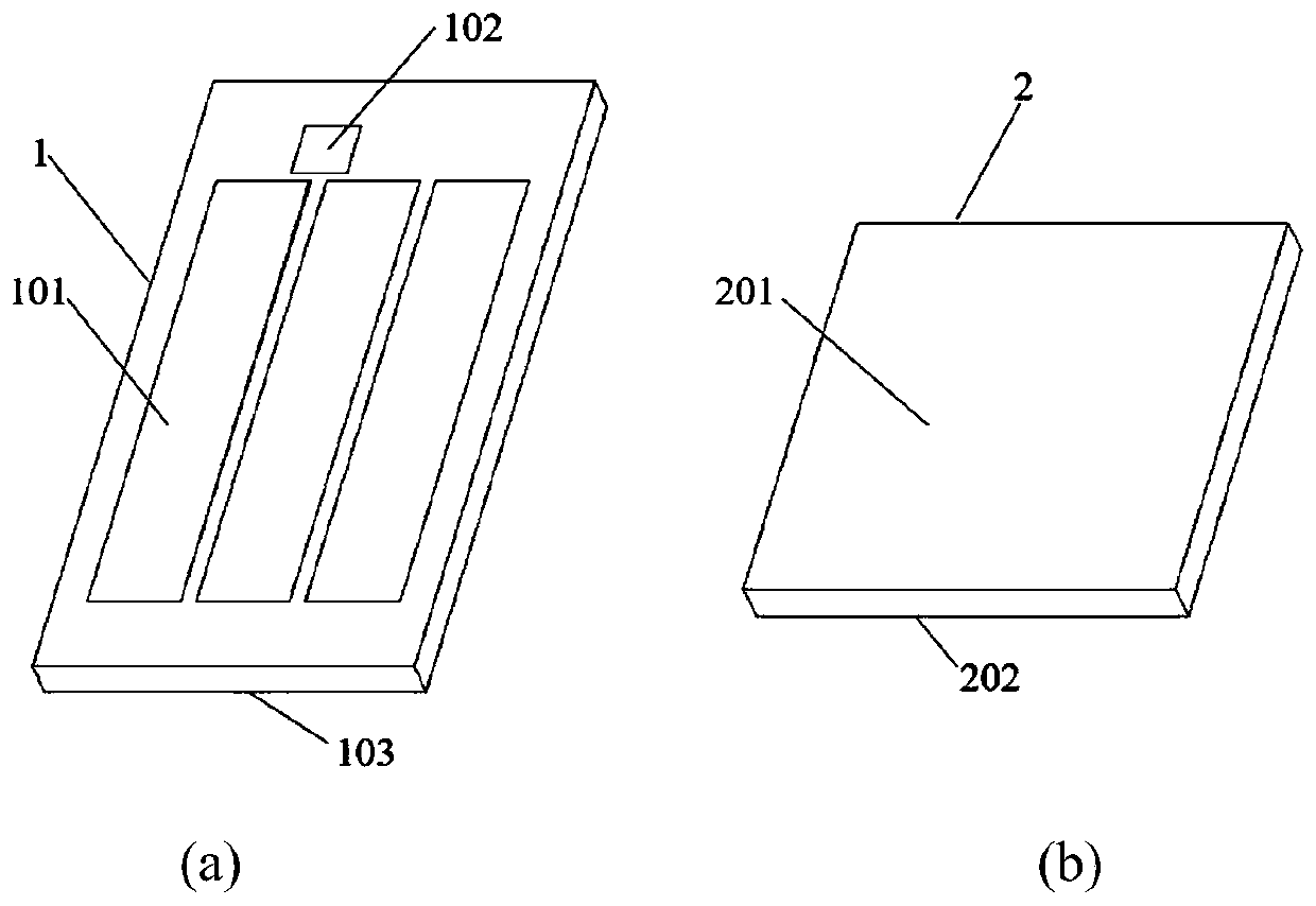
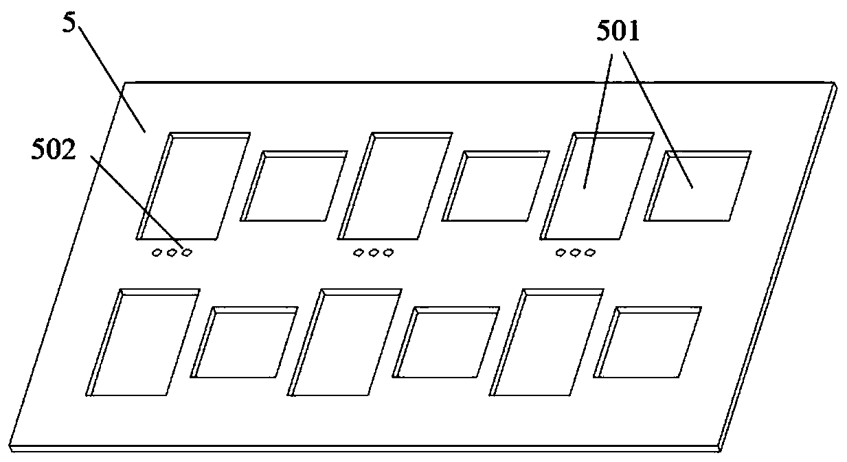
[0053] Such as figure 1 As shown, the invention discloses a packaging structure of an embedded double-sided interconnection power module, which consists of an IGBT power chip (1), a diode chip (2), an upper DBC substrate (3), a lower DBC substrate (4), a middle Interposer board (5), dielectric fill layer (6), solder layer (7), redistribution layer (8), via conductive metal (9), positive terminal (10a), negative terminal (10d), gate terminal sub (10b) and the common terminal (10c). The IGBT power chip (1) has an emitter (101) ...


PUM


Abstract

The invention discloses an embedded double-sided interconnection power module packaging structure and a manufacturing method. The embedded double-sided interconnection power module packaging structureis composed of an IGBT power chip, a diode chip, an upper DBC substrate, a lower DBC substrate, an intermediate adapter plate, a dielectric filling layer, a solder layer, a rewiring layer, via hole conductive metal and power terminals. According to the invention, the IGBT power chip and the diode chip are connected with the lower DBC substrate through the solder layer; meanwhile, a rectangular frame is manufactured on the intermediate adapter plate, and the IGBT power chip and the diode chip are embedded into the intermediate adapter plate by filling dielectric materials; the upper surfaces of the chip and the adapter plate are coated with conductive metal layers; the upper surface and the lower surface of the intermediate adapter plate are interconnected with the upper DBC substrate andthe lower DBC substrate respectively; and the power terminals are led out from the conductive copper-clad layers of the upper DBC substrate and the lower DBC substrate to obtain an embedded double-sided interconnection power module. According to the invention, double-sided heat dissipation of the IGBT power module can be realized, and the heat dissipation efficiency is improved; and bonding wiresare not used, so that the parasitic inductance of the module is reduced.

Description

technical field [0001] The invention relates to the technical field of packaging of power electronic devices, in particular to a packaging structure and a manufacturing method of an embedded double-sided interconnection power module. Background technique [0002] With the continuous development of power electronics technology, power modules have been more and more widely used in aerospace, rail transit, new energy vehicles, wind power generation, photovoltaic power generation and other industries. Currently, the mainstream power module on the market is the IGBT power module. The packaging of the traditional IGBT power module is mainly to weld the collector of the power chip and the anode of the diode chip connected in antiparallel to the copper-clad ceramic substrate (DBC) through lead-free solder, and then use wire bonding to realize the connection between the chip and the anode. Electrical interconnection between chips and between chips and DBC board. The copper substrat...

Claims


Application Information

Patent Timeline
Patent Type & Authority Applications(China)
IPC IPC(8): H01L23/538H01L25/18H01L23/367H01L21/60
CPCH01L23/367H01L23/5386H01L24/83H01L25/18H01L2224/83
Inventor 秦飞赵帅代岩伟陈沛安彤
Owner BEIJING UNIV OF TECH
Why Eureka
Try Eureka